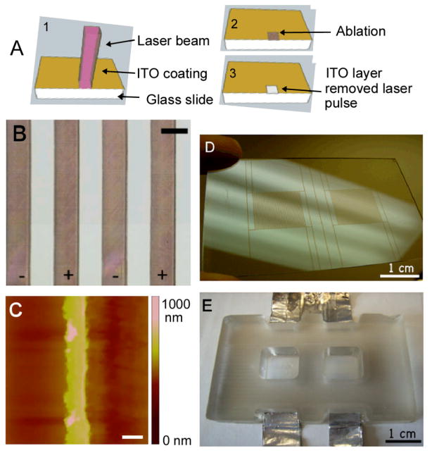
Figure 1. Indium-tin-oxide patterned substrate.
(A) Schematic of the laser-ablation process of the indium-tin-oxide substrates. (B) Closeup image of patterned electrode array with 200 μm electrodes and 200 μm spacing (scale bar corresponds to 200 μm). (C) Atomic force micrograph of a 50 μm-wide electrode patterned via laser ablation (scale bar: 50 μm) (D) Photograph of slide patterned with two interdigitated electrode arrays. (E) Photograph of bioreactor with two culture wells (employed for all studies reported here).

