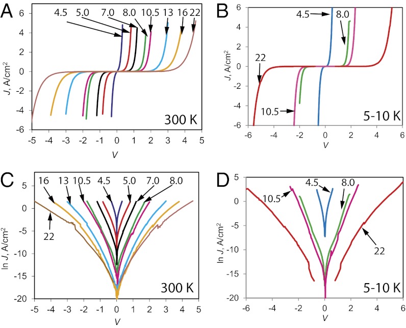
Fig. 1.
Current density vs. voltage (JV) curves for PPF/BTB/e-C/Au molecular junctions with BTB layer thickness indicated on each curve in nanometers. In all cases, the top contact consisted of 10 nm of carbon (e-C) and 15 nm of Au deposited by electron-beam evaporation at ∼5 × 10⁻⁷ torr. PPF is pyrolyzed photoresist film with covalent bonding to BTB layer, described previously (14, 34) (SI Appendix, section 2). JV curves were obtained with a four-wire geometry to correct for lead resistance. A and C were obtained at 300 K in air, whereas B and D were obtained at <10 K in vacuum.

