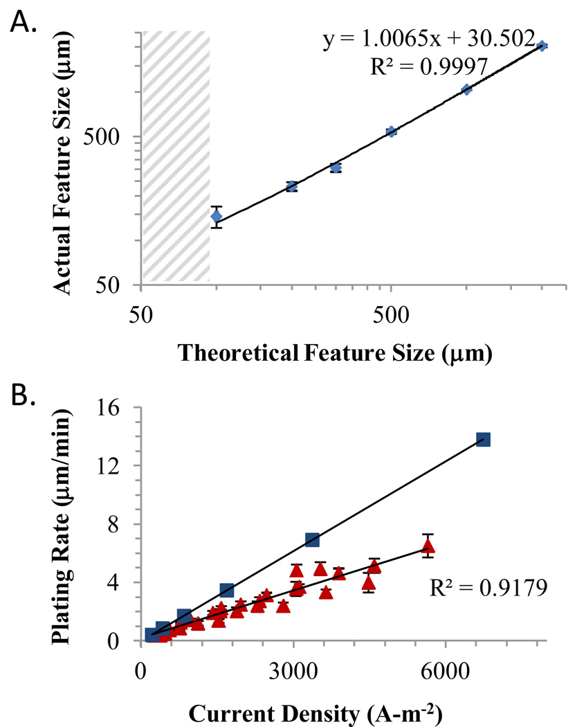
Figure 2.
(A) Plot showing a linear correspondence between final nickel feature resolution and the CAD design above 100 µm; below 100 µm the plotter fails to produce distinct features (gray hatching). The resolution is limited by the 10 µm resolution of the plotter and the stability of the vinyl sticker during cutting. (B) Plot of electroplating rate as a function of current density for a wide range of feature shapes and areas (triangles). The experimental plating efficiency is 53% relative to the theoretical limit (squares). All error bars show standard deviation of the mean.

