

Abstract
Slow light with a markedly low group velocity is a promising solution for optical buffering and advanced time-domain optical signal processing. It is also anticipated to enhance linear and nonlinear effects and so miniaturize functional photonic devices because slow light compresses optical energy in space. Photonic crystal waveguide devices generate on-chip slow light at room temperature with a wide bandwidth and low dispersion suitable for short pulse transmission. This paper first explains the delay-bandwidth product, fractional delay, and tunability as crucial criteria for buffering capacity of slow light devices. Then the paper describes experimental observations of slow light pulse, exhibiting their record high values. It also demonstrates the nonlinear enhancement based on slow light pulse transmission.
Keywords: slow light, photonic crystal, optical buffer, photonic router, optical nonlinearity
1. Introduction
Photonic packet routers are considered to be in-dispensable at network nodes in future optical fiber communication systems. The key device for them is an optical buffer, which controls the delay of optical signals and manages the timing of sending optical packets. But still it is difficult to realize on a chip because of ultrafast transmission of optical signals. The combination of an optical switch and fibers or waveguides of different lengths provides a digitally tunable delay. However, only mechanically movable optics that physically change the optical path length with a millisecond order response time are in practical use as a continuously tunable delay line. Slow light with a markedly low group velocity υg has been extensively studied toward a compact delay line with fast and continuous tunability.1),2) Also, slow light compresses optical energy in space and increases light-matter interaction, resulting in enhanced gain and absorption, phase shift, and nonlinearities. Main targets of early studies on slow light were to observe an ultralow group velocity and a long delay. In these years, they have shifted to realization of a wide bandwidth and low higher-order dispersion, which are essential and crucial for practical use of slow light; slow light pulses that carry and store information cannot be generated without them. In addition, tunability of slow light pulses, one of the final targets of this research, has been achieved recently.
In this paper, we first explain the principle of slow light and some important criteria for evaluating its performance. Then we describe two solutions of the issues of slow light using photonic crystal waveguides and some recent experimental demonstrations of the tunable delay and nonlinear enhancement.
2. Generation of slow light and issues
In general, slow light occurs due to large first order dispersion dk/dω arising from the resonance of light with a material or structure, where k is the wave number and ω is the angular frequency. As usually seen in textbooks on optics,3) the group velocity υg is given as (dk/dω)−1.
The most noticeable method that uses the material dispersion is the electromagnetically induced transparency (EIT).4) Using the resonance of light with electronic states in a vapor or solid, υg is reduced to more than eight orders of magnitude lower than the vacuum velocity of light c. In any slow light, the resonance brings a constraint between the delay Δtd and the frequency bandwidth Δf. A simple consideration gives the relation2)
| [1] |
where f is the center frequency, Δn is the change of material index in the bandwidth, ng ≡ c/υg is the group index denoting the slow down factor compared to c, and L is the device length. The inverse proportional relation of Δf and Δtd suggests that a long delay is only obtained for slowly varying optical signals with a narrow bandwidth. The extremely low υg in EIT only allows a bandwidth of the order of kHz. Furthermore, all the bandwidth is not usable because of higher order dispersion. The second order dispersion known as the group velocity dispersion (GVD), which expands the pulse width, becomes zero at the center frequency, but increases rapidly with a small frequency offset. The third and higher order dispersion that split the pulse are usually very large all over the bandwidth. Therefore, the usable bandwidth is limited to around the center, but still some distortion in pulse shape occurs. In most EITs, a gas cell and high performance refrigerator such as laser cooler, enabling an ultralow temperature less than 1 μK, are necessary to suppress the Doppler effect of gas and stabilize the electronic states. Thus, EIT devices are difficult to use as on-chip optical buffers. In these years, semiconductor optical amplifiers and silica fibers are studied as slow light devices operating at room temperature. The former uses the dispersion accompanied by gain and absorption. The latter uses the dispersion accompanied by the stimulated Raman scattering (SRS) and stimulated Brillouin scattering (SBS), or uses the dispersion in a highly dispersive fiber whose delay is selected by using parametric wavelength conversion.5) Their tunable delay is of ps order and/or the bandwidth is limited to less than 10 GHz.
For structural dispersion methods, Eq. [1] is still valid except that Δn is defined not for a material index but for an equivalent index of mode distributing over multiple materials that form the structure. Therefore, structural dispersion methods have similar problems in terms of the bandwidth and dispersion, although they are suitable for room temperature on-chip buffering.2) For example, a long delay of ns to μs order has been demonstrated using microsphere cavities with an extremely high quality factor Q of 106–108, but the bandwidth is reasonably narrow. Coupled resonator optical waveguides (CROWs) are effective for expanding the bandwidth.6),7) For example, more than one hundred microrings and photonic crystal microcavities are coupled in series, and a 100 ps order delay is obtained with a 10 GHz order bandwidth. Here, the cavities must have the same resonant wavelength so that light passes through all of them. It requires a severe structural uniformity particularly when Q of each cavity is very high. A small fluctuation results in a large spectral oscillation and limits the usable bandwidth to less than several GHz. The tunable delay requires external control of the coupling strength between neighboring cavities. But it is generally difficult as it requires a large local change of material index. All pass filters (APFs) are known as similar structures that give a wideband delay.6) They consist of many microcavities, each of which is coupled with a bass waveguide. Light is delayed by repeating the coupling and decoupling with cavities. It does not require the perfect matching of resonant wavelengths of cavities, while the bandwidth is narrowed by the multiplication of transfer functions of all the cavities. Photonic crystal waveguides (PCWs), the main topic of this paper, forms standing waves on the Bragg condition of their periodic structure (usually called band edge) and slow light occurs due to large first order dispersion near the Bragg condition.8) Presently, it is straightforward to observe experimentally a group velocity of c/10 – c/100 and a delay of 10 ps order. Similarly to the above, it is not applied for optical buffering as it is because of the bandwidth and dispersion issues.
3. Performance of slow light
From the constraint of the delay and bandwidth in Eq. [1], the delay-bandwidth product ΔtdΔf is used as a criterion for the potential buffering capacity as follows:2),9)
| [2] |
where λ is the wavelength in vacuum. Equation [2] is transformed using the relation ng= L/Δtd as follows:
| [3] |
As this equation is dimensionless, we can call it the normalized delay-bandwidth product. It is effective for fairly evaluating the potential buffering capacity of different length devices. It is seen that Δn is a crucial parameter for high performance slow light. A large Δn is achievable when the structure consists of high index contrast media such as semiconductor and air, and so the equivalent modal index changes widely depending on modal distributions.
Let us assume a Gaussian pulse as one-bit optical signal, and denote the full width at half maximum (FWHM) of the pulse and its frequency spectrum as Δτ and Δf, respectively. Then, the time-bandwidth product ΔτΔf = 2 · ln2/π = 0.441. If the FWHM of the pulse is assumed to be the interval between signals, the potential buffering capacity defined as Δtd/Δτ is given by 2.27 ΔtdΔf. But the net buffering capacity is smaller than this value because the pulse width Δτ is expanded by the higher order dispersions. The net capacity is usually evaluated by the fractional delay Δtd/Δτo, where Δτo is the output pulse width affected by the higher order dispersion. The fractional delay directly gives the number of pulses that are effectively stored in the device.
The delay-bandwidth product and fractional delay are the criteria for fixed buffering capacities. A more important criterion for buffering is the tunable delay by some external control. For the tunable delay Δtc, the tunable fractional delay Δtc/Δτo could be used as a criterion. However, such a tunable delay has been difficult in structural dispersion methods; a sole experimental demonstration was that exploiting the band edge shift against heating of a simple PCW.10) This method can be only applied to narrow band highly dispersive slow light. The tunability Δtc is not explicitly evaluated but estimated to be less than 1 ps.
Figure 1 summarizes the delay-bandwidth product of slow light from various sources.1) Most studies reported a value lower than 10 because they mainly focused the long delay, ignoring the bandwidth. Also, the maximum fractional delay has been less than 10. Recently, modified PCWs have achieved a delay-bandwidth product of over 100, fractional delay of 80 and tunable fractional delay of 22 using a concept that controls the chirping of the device, as shown below.
Fig. 1.
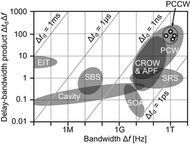
Relation of delay-bandwidth product and bandwidth of slow light from various sources. Circular plots of PCCW correspond to experimental results in Fig. 6.
4. Photonic crystal waveguides and dispersion control
Currently, most standard PCWs employ a photonic crystal slab consisting of high index slab with airhole array as a platform. It exhibits the photonic band gap for light polarized and propagating parallel to the slab plane. Light of this polarization often called TE-like is confined and guided by removing a row of airholes from the photonic crystal slab to form a line defect. Periodicities normal and parallel to the line defect primarily contribute to the optical confinement utilizing the photonic band gap and the generation of slow light, respectively. Here, slow light is intrinsically loss-less over the entire frequency band of slow light. It is an important advantage when considering that slow light in most of structures based on cavities is affected by the intrinsic radiation loss at the center frequency and by the intrinsic reflection loss at other frequencies in the slow light band. In addition, the delay simply increases as the device is elongated. It is the second and more practical advantage, compared with other structures, which are technically difficult to elongate. The detailed slow light characteristics are estimated from the photonic band diagram displaying the dispersion relation between ω and k. In general, the photonic band is distorted and flattened in the vicinity of its band edge in any periodic structures, resulting in the convergence of (dk/dω)−1 to zero and the generation of slow light. Here, Δk = Δn(2πf/c) becomes particularly large for a small Δf. We would skip the detail, but the frequency f of the guided mode is usually located around a frequency of 0.3c/a, and the maximum Δk reaches 0.20(2π/a) for the lattice constant a of the photonic crystal. Therefore, from Eq. [3], a large Δn of 0.6–0.7 can be expected. But the effective Δn is nearly half of this value as remarkable slow light only occurs near the band edge.
The fact that slow light only occurs near the band edge and arises from the distortion of the photonic band suggests the issues of the narrow bandwidth and higher order dispersions (particularly GVD), respectively. To solve these issues, we have proposed and studied two different concepts, dispersion-compensated slow light11) and low-dispersion slow light,12) as schematically illustrated in Fig. 2. For dispersion-compensated slow light, a photonic band showing a flat band and sandwiched by the opposite GVD characteristics is used. By changing structural parameters along the waveguide to form a chirped structure, the photonic band is shifted with position. When a short optical pulse is incident on such a device, each wavelength component of the pulse is slowed down and delayed at different position, and the GVD is compensated in total after passing through the opposite GVD areas. For a larger chirp slope, Δf is increased while Δtd is reduced because the overlap length of each wavelength component with the flat band is shortened. This means that the delay-bandwidth product still constrains slow light in chirped structures. In other words, external control of the chirp slope changes the bandwidth and delay. On the other hand, for the low-dispersion slow light, the standard PCW structure is minutely modified so that the photonic band exhibits a straight part simultaneously with a small slope. In general, the photonic band of the guided mode in the PCW arises from the anti-crossing of index confinement mode and bandgap confinement mode. The former is mainly dependent on the structure of the line defect, and the latter, the photonic crystal itself. A good balance between these two gives the straight slow light band.
Fig. 2.
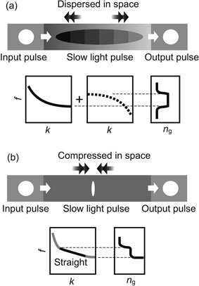
Schematics of two types of wideband dispersion-free slow light. (a) Dispersion-compensated slow light. (b) Low-dispersion slow light.
5. Dispersion-compensated slow light
An example device exhibiting dispersion-compensated slow light is the chirped photonic crystal coupled waveguide (PCCW), as shown in Fig. 3(a).13),14) It consists of two PCWs separated by three rows of airholes, where size and position of some airholes are slightly changed. In the photonic band diagram of Fig. 3(b), even and odd symmetric modes arising from the coupling of these PCWs appear. When the PCCW is connected with input and output PCWs through symmetric branch and confluence, as shown in Fig. 3(a), only the even symmetric guided mode is excited. This mode exhibits a flat band at an inflection point sandwiched by the opposite GVD characteristics. Wideband dispersion-compensated slow light explained in Section 4 is obtained by adding a chirped structure to the PCCW. The PCCW in Fig. 3(a) is designed to operate at C band (λ = 1.530 − 1.565 μm) of silica optical fiber communications. The device is fabricated on silicon-on-insulator substrate with the top Si slab of 0.21 μm thickness by using e-beam lithography, SF6 inductively coupled plasma reactive ion etching, and HF wet etching. The length of the PCCW in this experiment is 250 μm. The band shifts from low to high frequencies in a chirped structure where the airhole diameter except on the center row is changed from 0.25 to 0.26 μm. To form smooth chirping, the exposure time of the e-beam lithography is gradually changed for the same designed diameter.
Fig. 3.
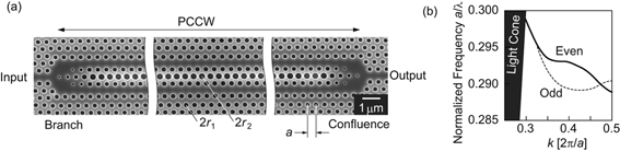
PCCW integrated with input/output PCW. (a) Top view of fabricated device on SOI substrate. 2r1 is chirped from 0.25 μm to 0.27 μm. 2r2 is fixed at 0.36 μm. (b) Photonic band diagram of PCCW.
Figure 4 shows three setups for measuring the slow light characteristics. In all of them, TE-polarized incident light is coupled to the waveguide using objective lenses. Output light is detected from above the device through another objective lens or from the lateral direction using lensed fiber. The transmission spectrum is simply measured using tunable laser and power meter. Although its detection efficiency is lower, the first detection scheme is used here to eliminate the direct coupling of incident light and assuring a large dynamic range of the spectrum. The group delay spectrum is measured using modulation phase shift method with the second detection scheme to acquire a higher detection efficiency. Here, tunable laser light is modulated at a frequency fm and transmitted through the device. The delay Δtd is evaluated from the phase shift Δϕ inside the device using the relation Δϕ = 2πfmΔtd. The pulse transmission is measured using mode-locked fiber laser whose pulse spectrum is controlled using wavelength- and bandwidth-tunable BPF. It is branched into two by a fiber coupler. One is inserted into the device and the other is used as a reference. The cross-correlation trace showing the pulse delay and higher order dispersion in the device is obtained from these two branches. Approximating the pulse shape to be Gaussian, the full-width at half-maximum (FWHM) of the output pulse from the device Δτo is evaluated using the relation Δτmes2 = Δτo2 + Δτref2, where Δτmes and Δτref are the FWHMs of the measured trace and reference pulse, respectively.
Fig. 4.
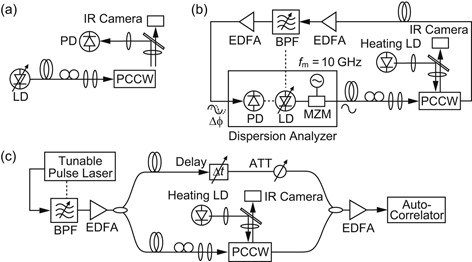
Measurement setups for (a) transmission spectrum, (b) group delay spectrum using modulation phase shift method, and (c) pulse transmission.
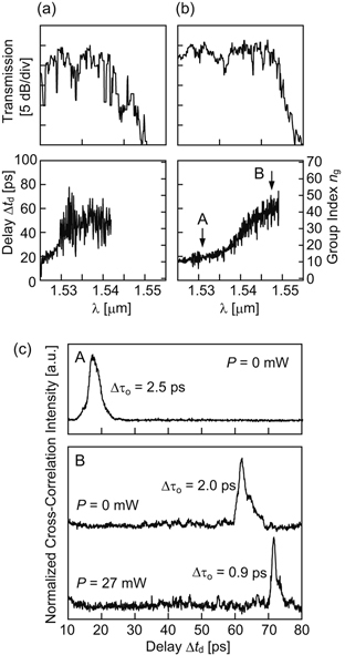
Figure 5(a) shows the measured transmission spectrum almost covering the C band except for the intensity dip at λ = 1.548 μm. The sum of the propagation loss in the PCCW and the connection loss at the branch and confluence is roughly estimated to be 5 dB. The spectral oscillation is caused by the internal resonance between the branch and confluence and/or the light localization due to disordering of the structure. Figure 5(b) shows the group delay spectrum measured using modulation phase shift method. The delay is 10–15 ps at λ < 1.547 μm, while increases to ∼40 ps at λ = 1.548 − 1.560 μm. Here, ng = 42, Δn = 0.32, and a delay-bandwidth product ΔtdΔf = 57 are estimated, which are in good agreement with those calculated from the band diagram and chirp slope.
Fig. 5.
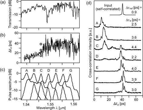
Transmission characteristics of PCCW. (a) Transmission spectrum. (b) Group delay characteristics measured by using modulation phase shift method. Circular plots show the delay obtained from those of optical pulse in (d). (c) Input pulse spectra. (d) Cross-correlation traces of output pulse and reference pulse. The top shows the auto-correlation trace of input and reference pulses. Pulse width Δτo was estimated by deconvoluting the cross-correlation trace of the output pulse from the reference pulse. In (b)–(d), A–G denote the same pulse spectra.
To confirm the delay and dispersion compensation, the short pulse transmission is also observed. Here, an optical pulse of 0.9 ps width from passively mode-locked fiber laser (40 MHz repetition frequency) is incident on the device. The center wavelength λp of the pulse is changed, as shown by symbols A–G in Fig. 5(c). The output pulse is observed over the slow light band with some distortion, as shown in Fig. 5(d). The pulse delay Δtd jumps from 10 to 40 ps at λp= 1.547 μm, and keeps constant in the slow light band. This result agrees well with that obtained by the modulation phase shift method. Roughly approximating the pulse shape as a Gaussian, Δτo is 3.3 ps on an average and the fractional delay is 12. The expansion and distortion in the pulse might be caused by the GVD and light localization due to structural disordering. But still GVD in this device is suppressed effectively in comparison with that of the band edge slow light in a simple PCW.
The similar characteristics were observed for longer devices up to 1 mm, as shown in Fig. 6. Here, the maximum delay is 173 ps for L = 1 mm, but a maximum ΔtdΔf of 110 is recorded for L = 800 μm. The delay-bandwidth product does not necessarily increase linearly with the device length. It might be due to disordering of the structure, which locally increased the loss and dispersion and reduced the effective bandwidth. In addition, the loss and dispersion increase linearly with L even in the effective bandwidth. Therefore, the pulse transmission was confirmed up to 800 μm with Δtd= 135 ps and Δτo= 5.5 ps, corresponding to a fractional delay of 25. To obtain higher values for longer devices, influence of the disordering must be suppressed.
Fig. 6.
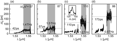
Delay spectra observed for L = (a) 250 μm, (b) 400 μm, (c) 800 μm, and (d) 1 mm. Discontinuity of spectra in (c) and (d) is due to low output power that disturbed the acquisition of reliable data. Gray bands denote the effective slow light band, in which moving average of data points is lying inside ±10% of the total average value. Gray dashed lines denote average delay in the effective band. The inset in (c) shows the cross-correlation trace of optical pulse with Δτref= 0.9 ps and Δτo= 5.5 ps. As the center wavelength of the pulse was set at 1.549 μm, Δtd increases from the average value indicated by the gray dashed line to 130 ps.
6. Tunable delay
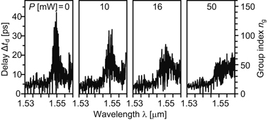
As noted in Section 4, the delay and group index of dispersion-compensated slow light can be controlled by changing the chirp slope.14) The device in Fig. 3 has the airhole diameter chirping. But any structural parameters that shift the photonic band are applicable to the chirping. The total amount of the chirping can also be controlled by changing the material index along the PCCW with the airhole diameter chirping. For example, local laser heating is carried out to slope the index of the Si slab by means of the temperature distribution. Blue-violet laser light at λ = 0.442 μm is used to obtain a high absorption efficiency at the Si slab. The laser spot is deformed to an elliptical profile (400 × 180 μm2) by using cylindrical and objective lenses. The slab index can be estimated from the resonant shift in photonic crystal nanocavities integrated adjacent to the PCCW. The linear increase in proportion to the laser power P and semi-exponential distribution of the temperature from the spot center are confirmed, and the maximum index change is evaluated to be as high as 0.11 at P = 50 mW. Figure 7 demonstrates the group delay characteristics suggesting the formation of the slab index chirping in a 90 μm long PCCW without the airhole diameter chirping. When no heating is carried out, the slow light band appears as a sharp peak due to the flat band in Fig. 3. The particularly large oscillation in the spectrum is caused by enhanced reflection at the branch and confluence in the unchirped structure under the slow light condition. When the heating is carried out, the index chirping is formed and the peak is suppressed and broadened to the long wavelength side. In addition, the slow light area is shifted to inside of the PCCW. It suppresses the reflection at the branch and confluence and the oscillation in the spectrum. Thus wideband slow light induced by the index chirping is realized.
Fig. 7.
Change of the delay and group index spectra against local heating at the branch of unchirped PCCW (2r1 = 0.25 mm), which was observed in modulation phase shift measurement.
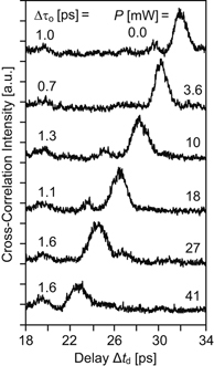
The spectral peak in Fig. 7 is too narrow to let the short optical pulses in Fig. 5(d) pass through the device. The mixture of the airhole diameter and slab index chirping is more suitable for the tunable delay of such sub-ps wide slow light pulse. Figure 8 shows the cross-correlation trace of output pulse from the same device as for Fig. 2, exhibiting an average Δτo of 1.2 ps.14) Changing power P, clear delay tuning of the slow light pulse is achieved in the range of Δtd= 31–23 ps (Δtc= 8 ps) with maintaining Δτo. This is the first demonstration of optical buffering action of on-chip slow light device with a tunable buffering capacity of 7.
Fig. 8.
Cross-correlation trace of output optical pulse from the chirped PCCW against local heating.
7. Folded chirping
Two simple ways to enhance the buffering capacity and its tunability are to elongate the device and to improve the heating efficiency. In longer devices, however, the slow light characteristics become more sensitive to structural disordering. When the device is elongated without changing the chirp range so that the bandwidth is maintained, the chirp slope is reduced and the disordering could locally invert the chirp direction. It gives rise to unwanted mode gaps and internal resonance around the slow light areas, resulting in large oscillation of transmission and delay spectra, as well as the local GVD. Such a situation can be improved by folded chirping, in which the direction of the chirping is intentionally inverted at positions not overlapping with slow light areas.15) It is advantageous because it gives the same delay for a larger chirp slope, suppressing the influence of the disordering. It is also effective for expanding the tuning range by the laser heating. For a monotonous index chirping described in Section 6, the laser spot is usually centered on one end of the PCCW, such that one half of the laser spot irradiates the PCCW, while the other half irradiates an area that does not affect the PCCW. In contrast, the folded chirping is formed easily by irradiating the whole laser spot around the device center, so that the spot intensity and hence the thermo-optic index change decreases away from the center. This doubles the chirp length and tuning range with the same heating power.
Figure 9(a) and (b) compare the transmission and delay spectra for the monotonous and folded chirping of the airhole diameter in a 400 μm long device, respectively. The folded chirping exhibits a 2–3 dB higher transmission intensity with smaller oscillation than those of the monotonous chirping. Accordingly, the delay increased with smaller oscillation. Figure 9(c) shows the cross-correlation trace of output pulse for the folded chirping. Compared with the reference pulse of Δτref= 0.9 ps, the output pulse in the slow light regime is slightly dispersed as Δτo= 2.0 ps. When slight heating is carried out, the delay increases and the pulse width narrows to 0.9 ps because the imperfect dispersion compensation in the device is canceled by the slightly nonlinear profile of the index chirping. On this condition, the delay is 72 ps, and the corresponding fractional delay Δtd/Δτo is as large as 80, which is the record high value for on-chip slow light devices.
Fig. 9.
Slow light characteristics of 400-μm-long chirped PCCW. (a) Transmission and delay spectra of monotonous-chirped device, and (b) those of folded-chirped device. (c) Normalized cross-correlation trace of output pulse, where A and B correspond to those in (b).
Optical pulses can pass through the device in the narrow slow light spectrum, when the pulse width is moderately broadened by filtering its spectrum before the input. Figure 10(a) and (b) show the pulse transmission through 280-μm-long device with the heating for two different pulse widths Δτref= 10.2 and 3.9 ps, respectively. In general, a narrower spectral width gives a long delay around the peak and a wider tuning range. For the wider pulse, the delay Δtd changes from 111 to 8 ps by changing the heating power P. Thus, the tuning range is 103 ps and the fractional tunability is 9 for an average pulse width Δτo of 11.4 ps. For the narrower pulse, the dispersion became severe during the tuning only with controlling P. Therefore, the center position of the heating, x, is optimized simultaneously with P so that the dispersion is minimized. As a result, a tuning range of 74 ps is observed for an average Δτo of 3.4 ps, indicating a larger fractional tunability of 22.
Fig. 10.
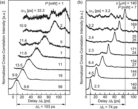
Delay tuning of different width slow light pulse. For (a), the center position of the heating, x, is fixed at the center of PCCW, i.e. 140 μm.
8. Low dispersion slow light and nonlinear enhancement
As noted in Section 4, higher order dispersions are eliminated in a straight photonic band when the line defect and photonic crystal of the PCW are optimized. 16)–18) Various structural parameters can be used as tuning parameters for this purpose. In most cases, however, fabrication of such structures is not straightforward because it requires a high accuracy with a less than 30 nm error simultaneously for multiple parameters. A lattice shift type structure, as shown in Fig. 11(a), is effective for simplifying this issue.19) Here, only the third rows of holes from the line defect are slightly shifted by an amount of s from their original positions along with the line defect. Calculated photonic bands for two different s/a and measured transmission characteristics for those fabricated into SOI substrate are shown in Fig. 11(b) and (c), respectively. The photonic band becomes straight even for a small s/a = 0.1, and the corresponding measured result exhibits a constant ng in the slow light band. Here, Δtd= 94 ps, ng= 60, and ΔtdΔf = 35 are obtained in a sample with L = 470 μm and s = 60 nm. The delay-bandwidth product is slightly smaller than that of dispersion-compensated slow light, because the range of the straight photonic band is limited. When s is increased to 80 nm, ng decreases while ΔtdΔf is enhanced to 53.
Fig. 11.
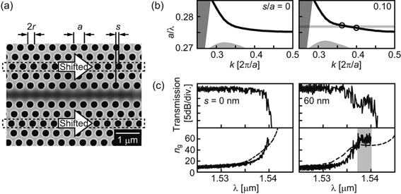
Low-dispersion slow light. (a) Top view of fabricated lattice-shifted PCW showing zero-dispersion slow light. (b) Calculated two-dimensional band of the guided mode for two s/a with an equivalent index of 2.9 and the transverse-electric polarization. The gray line and circles denote zero-dispersion slow light. (c) Measured transmission characteristics for two s. The gray region and dashed line denote zero-dispersion slow light and the calculated group index, respectively.
When an optical pulse similar to that in Fig. 5 is inserted into such a waveguide, an output pulse of Δτo = 2.4 ps is observed. Different from dispersion-compensated slow light, the low-dispersion slow light pulse is compressed in space just after it is incident on the waveguide. Here the pulse waveform is maintained and its peak intensity is enhanced in proportion to ng. Therefore, it is effective for nonlinear enhancement. Figure 12 shows the intensity characteristics measured for two different samples exhibiting ng= 8 and 30. The experimental plots agreed with theoretical lines with two photon absorption (TPA) coefficients β = 6 cm/GW and 25 cm/GW, respectively. They are 10 and 42 times higher than 0.6 cm/GW reported for Si photonic wire waveguides having strong optical confinement similar to that of the photonic crystal waveguide. The enhancement is almost proportional to ng2, which suggests that the enhancement is attributed to the slow light effect. Here, the free carrier absorption induced by the TPA might increase the local temperature. But it does not affect the slow light characteristics because the slope of the straight photonic band is kept constant against the simple band shift with heating. Simultaneously with the TPA, the spectral broadening due to self-phase modulation is also observed to be enhanced by the slow light effect. Also, the third harmonic generation enhanced by this effect allows the green emission from the waveguide.20)
Fig. 12.
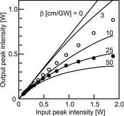
Intensity response of zero-dispersion PCW. Solid lines are the calculation results for different effective TPA coefficients β. The open and closed circles denote the experimental results for two PCWs exhibiting ng ∼ 8 and 30, respectively.
9. Summary
Slow light technology based on photonic crystal waveguides are making progress rapidly in these years. In particular, the slow light pulse is easily obtained by moderately expanding its bandwidth and suppressing the higher order dispersion. It enables us to observe various effects associated with slow light. Continuously tunable delay in dispersion-compensated slow light enables advanced and/or novel time-domain optical signal processing. For this purpose, a higher tuning mechanism than the heating, such as carrier plasma effect and electro-optic effect, will be an important issue to be investigated in the photonic crystal slab. In addition, group-velocity-dependent loss is a severe problem, although it was not discussed in detail in this paper.21) A more robust structure against disordering is desired toward practical applications.
Profile
Toshihiko Baba was born in Nagano in 1962. He received the B.E., M. E. and Ph. D. Degrees all from the Division of Electrical and Computer Engineering, Yokohama National University (YNU), Japan, in 1985, 1987, and 1990, respectively. During the Ph. D. work, he had been engaged in ARROW waveguides and on-Si photonic integration. From 1991–1993, he joined Tokyo Institute of Technology as a research associate. He discussed the spontaneous emission control in VCSELs and achieved the room temperature cw operation in devices at fiber communication wavelengths. He became an associate professor and full professor of YNU in 1994 and 2005, respectively. In these 15 years, he has studied photonic nanostructures such as photonic crystals (PCs), high-index-contrast structures, and Si photonics. He first demonstrated PC waveguides, surface-PC LEDs, and Si photonic wire components. He also achieved the room temperature cw operation in PC nanolasers and microdisk lasers, record high single-mode power PC-VCSEL, negative refractive components, and ultra-compact Si AWG demultiplexer. His recent studies focus on slow light in PC waveguides towards optical buffering and nonlinear enhancement. He is the author of ∼140 journal papers, which have been cited more than 3300 times in total, and has been served as the invited speaker at 93 international conferences. Dr. Baba is a member of the Institute of Electronics, Information and Communication Engineers (IEICE), the Japan Society of Applied Physics, the Institute of Electrical and Electronics Engineering (IEEE) Photonics Society, Optical Society of America and American Physics Society. He is one of the founders of International Workshop on Photonic and Electromagnetic Crystal Structures (PECS) in 1999. He is now chairing IEICE Silicon Photonics Committee. He received nine academic awards including JSPS Award in 2005 and IEEE LEOS Distinguished Lecturer Award in 2006–2007.

References
- 1).Parra E. and Lowell J.R. (2007) Toward applications of slow light technology. Opt. Photon. News 18, 40–45 [Google Scholar]
- 2).Baba T. (2008) Slow light in photonic crystals. Nat. Photonics 2, 465–473 [Google Scholar]
- 3).Saleh B.E.A. and Teich M.C. (2007) Fundamentals of Photonics Second Ed. Wiley, New Jersey [Google Scholar]
- 4).Hau L.V., Harris S.E., Dutton Z. and Behroozi C. H. (1999) Light speed reduction to 17 metres per second in an ultracold atomic gas. Nature 397, 594–598 [Google Scholar]
- 5).Thevenaz L. (2008) Slow and fast light in optical fibres. Nat. Photonics 2, 474–481 [Google Scholar]
- 6).Xia F., Sekaric L. and Vlasov Y. (2007) Ultracompact optical buffers on a silicon chip. Nat. Photonics 1, 65–71 [Google Scholar]
- 7).Notomi M., Kuramochi E. and Tanabe T. (2008) Large-scale arrays of ultrahigh-Q coupled nanocavities. Nat. Photonics 2, 741–747 [Google Scholar]
- 8).Notomi M., Yamada K., Shinya A., Takahashi J., Takahashi C. and Yokohama I. (2001) Extremely large group-velocity dispersion of line-defect waveguides in photonic crystal slabs. Phys. Rev. Lett. 87, 253902. [DOI] [PubMed] [Google Scholar]
- 9).Tucker R. S., Ku P-C. and Chang-Hasnain C. J. (2005) Slow-light optical buffers – capabilities and fundamental limitations. J. Lightwave Technol. 23, 4046–4066 [Google Scholar]
- 10).Vlasov Y.A., O’Boyle M., Hamann H.F. and McNab S.J. (2005) Active control of slow light on a chip with photonic crystal waveguides. Nature 438, 65–69 [DOI] [PubMed] [Google Scholar]
- 11).Mori D. and Baba T. (2004) Dispersion-controlled optical group delay device by chirped photonic crystal waveguides. Appl. Phys. Lett. 85, 1101–1103 [Google Scholar]
- 12).Sakai A., Kato I., Mori D and Baba T. (2004) Anomalous low group velocity and low dispersion in simple photonic crystal line defect waveguides. Tech. Dig. IEEE/LEOS Annual Meet., ThQ5 [Google Scholar]
- 13).Mori D. and Baba T. (2005) Wideband and low dispersion slow light by chirped photonic crystal coupled waveguide. Opt. Express 13, 9398–9408 [DOI] [PubMed] [Google Scholar]
- 14).Baba T., Kawasaki T., Sasaki H., Adachi J. and Mori D. (2008) Large delay-bandwidth product and delay tuning of slow light pulse in photonic crystal coupled waveguide. Opt. Express 16, 9245–9253 [DOI] [PubMed] [Google Scholar]
- 15).Adachi J., Ishikura N., Sasaki H and Baba T. (2009) Record wide range tuning of slow light pulse in photonic crystal coupled waveguide via turnup chirping. OSA Slow and Fast Light Top. Meet., SWA1 [DOI] [PubMed]
- 16).Frandsen L.H., Lavrinenko A.V., Fage-Pedersen J. and Borel P.I. (2006) Photonic crystal waveguides with semislow light and tailored dispersion properties. Opt. Lett. 14, 9444–9446 [DOI] [PubMed] [Google Scholar]
- 17).Kubo S., Mori D. and Baba T. (2007) Low-group-velocity and low-dispersion slow light in photonic crystal waveguides. Opt. Lett. 32, 2981–2983 [DOI] [PubMed] [Google Scholar]
- 18).Li J., White T.P., O’Faolain L., Gomez-Iglesias A. and Krauss T.F. (2008) Systematic design of flat band slow light in photonic crystal waveguides. Opt. Express 16, 6227–6232 [DOI] [PubMed] [Google Scholar]
- 19).Hamachi Y., Kubo S. and Baba T. (2009) Slow light with low dispersion and nonlinear enhancement in a lattice-shifted photonic crystal waveguide. Opt. Lett. 34, 1072–1074 [DOI] [PubMed] [Google Scholar]
- 20).Corcoran B., Monat C., Grillet C., Moss D.J., Eggleton B.J., White T.P.et al. (2009) Green light emission in silicon through slow-light enhanced third-harmonic generation in photonic-crystal waveguides. Nat. Photonics 3, 206–210 [Google Scholar]
- 21).Engelen R.J.P., Mori D., Baba T. and Kuipers L. (2008) Two regimes of slow-light losses revealed by adiabatic reduction of group velocity. Phys. Rev. Lett. 101, 103901. [DOI] [PubMed] [Google Scholar]