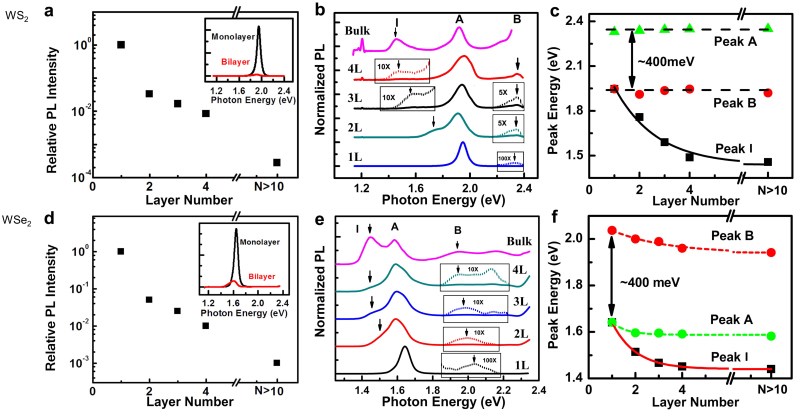
Figure 3.
(a) and (d): The relative PL intensity of WS2 (a) and WSe2 (d) multilayers respectively as a function of film thickness under the same conditions (normalized by the PL intensity of monolayer at 1). Insets present PL spectra from WS2 (a) and WSe2 (d) monolayers and bilayers respectively. The spectra were taken at the same conditions (excitation power, exposure time, etc.); (b) and (e): The normalized PL spectra (with respect to the peak A) of WS2 (b) and WSe2 (e) ultrathin films. I labels the luminescence from indirect gap interband transition, A and B label the direct-gap transitions from the split valence band edge to the conduction band edge at K points (see text). Spectra (dash line) in the zoom windows have been multiplied by a factor as indicated for clarity; (c) and (f): The peak positions of I, A and B transitions as a function of the film thickness in WS2 (c) and WSe2 (f). Both cases show a nearly constant energy difference of ~0.4 eV which corresponds to the splitting of the valence band edge. The universal A-B splitting implies a suppression of interlayer hopping in tungsten dichalcogenides ultrathin thin films.

