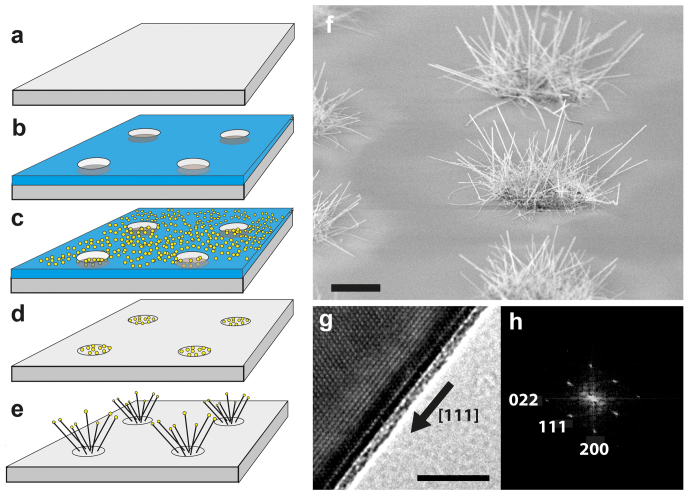
Figure 1. Fabrication and characterization of silicon nanowires (NWs) on glass.
(a) Microscope cover slips (b) were patterned with optical lithography to (c) locally deposit 40 nm Au colloids in micropatterned arrays. (d) Au colloids on separated islands served as (e) nucleation catalysts to grow randomly oriented silicon nanowires. (f) The SEM micrograph shows in bird's eye view the micropatterned islands of Vapor-Liquid-Solid (VLS) grown silicon nanowires with length of 5-10 μm and 40 nm in diameter. (g) Single crystallinity of NWs was confirmed by high-resolution transmission electron microscopy (TEM). The crystal orientation is <111> along the SiNW growth axis as indicated by the black arrow. Silicon has an anisotropic modulus of elasticity depending on the crystal orientation. The elastic modulus of Si along the <111> orientation is 169 GPa, which is used for calculation of NW spring constants. A 1–2 nm thin native amorphous SiO2/SiOx layer is clearly visible on the NW surface in the TEM micrograph. (h) The crystal orientation was determined from TEM images with “CRSIP” software for advanced crystallographic analysis. Scale bars f = 5 μm, g = 5 nm.

