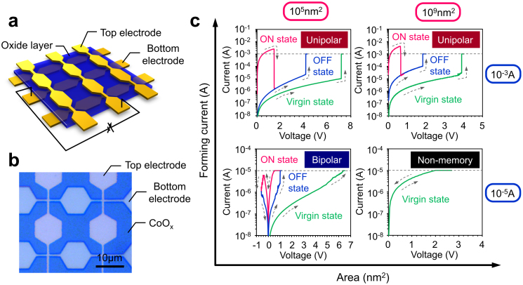
Figure 1. Schematic of typical resistive switching device, the fabricated structure of Pt/CoOx/Pt, and their typical current-voltage (I–V) data.
(a) Schematic of resistive switching cross-bar junction device, (b) SEM image of fabricated resistive switching devices of Pt/CoOx/Pt, (c) I–V data when varying the forming current and the cell area. Data of the forming current of 10−5 A and the cell area of 105 nm2, the forming current of 10−3 A and the cell area of 105 nm2, the foming current of 10−5 A and the cell area of 109 nm2 and the forming current of 10−3 A and the cell area of 109 nm2 are shown in the figure.

