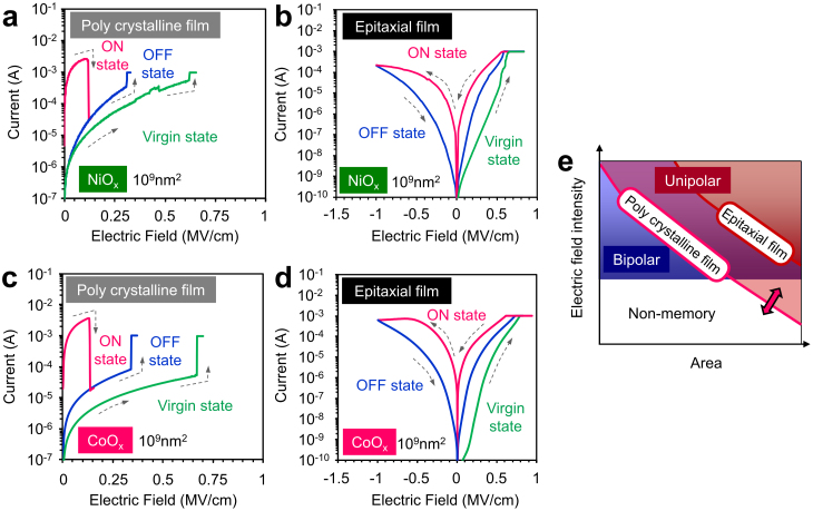
Figure 4. Comparison between an epitaxial film device and a polycrystalline device on the resistive switching behaviors.
(a) I–V data with the forming current of 10−3 A and the cell area of 109 nm2 for polycrystalline NiOx device. (b) I–V data with the forming current of 10−3 A and the cell area of 109 nm2 for epitaxial single crystalline NiOx device. (c) I–V data with the forming current of 10−3 A and the cell area of 109 nm2 for polycrystalline CoOx device. (d) I–V data with the forming current of 10−3 A and the cell area of 109 nm2 for epitaxial single crystalline CoOx device. (e) Diagram to explain why single crystalline device tends to exhibit a bipolar switching even for relatively large cell areas.

