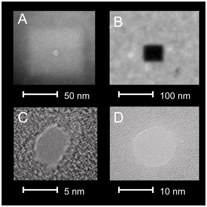
Figure 1. TEM images of nanopores.
(A) A bright-field TEM image of a thinned silicon nitride region with a small nanopore; (B) A high-angle annular dark field scanning TEM (HAADF-STEM) image of a thinned nitride region; (C) A TEM bright-field image of an ~3 nm-diameter nanopore in a silicon-nitride membrane; (D) A TEM bright-field image of an ~10 nm diameter nanopore in a silicon nitride membrane. All images were taken using a Technia F-20 S/TEM instrument.

