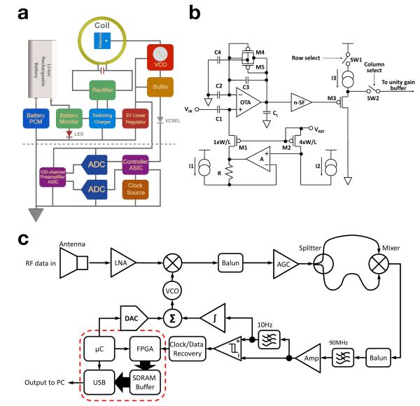
Figure 4.
Electronic schematics of neural interface, amplification circuitry, and telemetry unit. (a) Block diagram of the implantable module, including AB and TxB. The TxB (above the dotted line) receives a TTL input from the AB (below the dotted line) that modulates a freely running commercial VCO. (b) The circuit block diagram of the 100-ch CMOS preamplifier ASIC is shown. The preamplifier uses a capacitive-feedback, folded cascode operational transconductance amplifier (OTA) configuration with a source follower output buffer. (c) The RF superheterodyne receiver (Rx) is shown using a polarized antenna to reduce the sensitivity to movement of the transmitter antenna.

