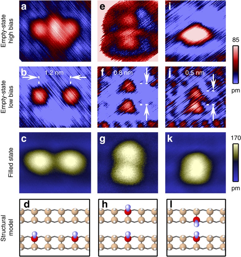
Figure 4. DB pairs with varying separation and orientation.
(a–d) Along a dimer row separated by two H-terminated lattice sites (1.9, 1.5, −1.5 V; 5 pA; 2.7 × 2.3 nm2); (e–h) across two dimer rows separated by a single H-terminated lattice site (2.2, 1.7, −2.0 V; 2 pA; 1.9 × 2.3 nm2); and (i–l) on adjacent sites across the dimer trough (2.0, 1.5, −2.0 V; 5 pA; 1.9 × 2.3 nm2). In each case, there is agreement with the behaviour of the DB pair described in Fig. 3; in particular, we see the formation of a protrusion between DB sites at high empty-state bias and low-tunnelling current due to the band alignment between the tip Fermi level and LBE of the DB structures as described in the text. Length measurements have associated uncertainties of ±0.1 nm. Panels d, h and l show top-view schematic ball and stick models for each configuration; silicon atoms with DBs are coloured red.

