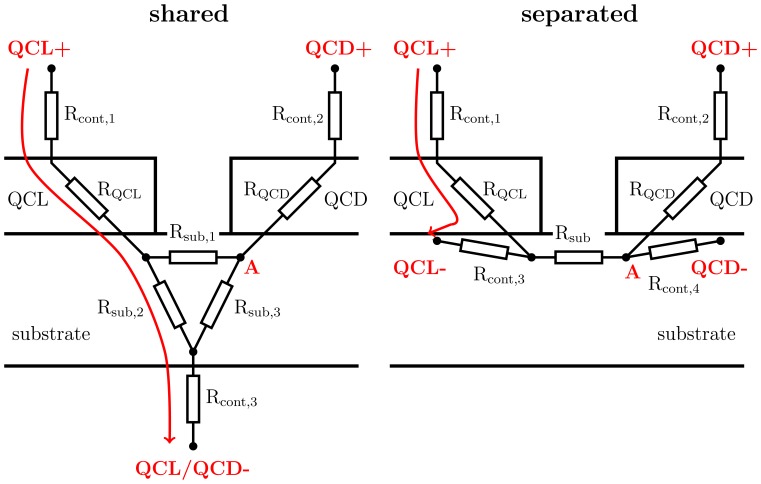
Figure 3.
Schematic DC circuit diagram of the device with a shared bottom-side contact (left) and separated bottom contacts (right). The laser bias voltage is indicated by a red arrow. Separated bottom contacts allow to minimize electrical crosstalk to the detector, as both detector contacts are affected in the same manner. Thus a potential fluctuation at node“A” cancel out.

