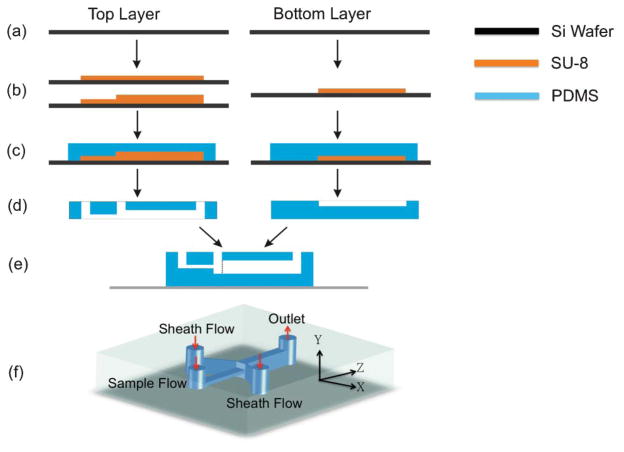
Fig. 2.
Process flow of 3D flow focusing device. (a) Si wafers as substrates for molds. (b) Forming double-step and single-step SU-8 molds. (c) Pour PDMS onto the SU-8 molds. (d) Remove PDMS from the mold. Inlet and outlet holes were punched in the top layer. (e) Two layers were bonded according to the directions in (d), with the bottom layer attached to a glass slide. (f) A view of the finished device. Coordinates are defined and will be used throughout the paper.

