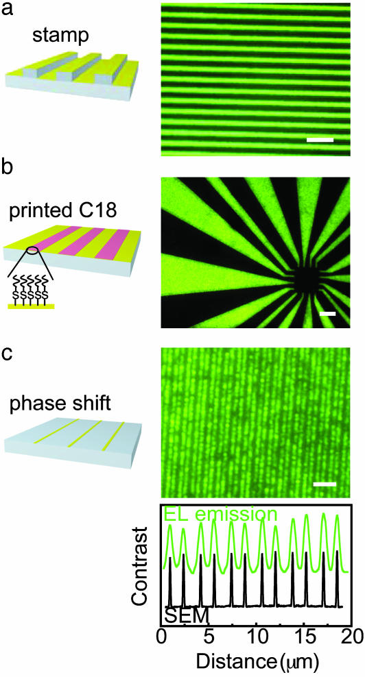
Fig. 4.
Patterned OLEDs formed by the combined use of ScL and soft lithography. In all cases, the Au was 20 nm thick and the electroluminescent layer was a polyfluorene derivative blended with 17 wt % of TBABF4 (100 nm). The unpatterned devices showed EL efficiencies of 0.65% ph/el. The schematic illustrations on the left show the modifications to the ScL electrodes, and the images on the right represent an example of OLEDs fabricated by using the approach. (a) Molding features of relief into the PDMS followed by blanket deposition of the electrode generates emission in the pattern of the raised features. (Scale bar, 100 μm.) (b) Microcontact printing an insulating self-assembled monolayer (octadecanethiol; C18) before lamination yields emission only in the bare Au regions. (Scale bar, 100 μm.) (c) Photolithography with a conformable phase mask followed by etching directly patterns lines (150 nm wide) of Au on the PDMS. The averaged linewidth (≈ 600 nm) of the pattern of emission (graph below) in this case is comparable to the resolution of the optical imaging system. (Scale bar, 5 μm.) The Rayleigh diffraction limit for the 0.55-numerical-aperture microscope objectives is 590 nm at a wavelength of 540 nm. The EL image was taken through the ITO (100 nm)/glass (0.4 mm), which reduces the effective numerical aperture.

