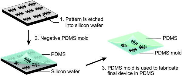
Figure 2.

Schematic overview of the three principal steps. (Step 1) The patterns are etched into a 4″ silicon wafer. (Step 2) The silicon wafer is used as a mold to fabricate the negative structures in PDMS. (Step 3) The PDMS mold is subsequently used to fabricate the final structures in PDMS. For simplicity we depict only 9 structures (whilst typically a wafer contains 24).
