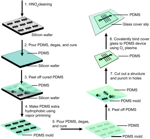
Figure 6.
Schematic of the fabrication of multiple structures in PDMS with sub-micron sized growth channels. (Step 1) The wafer is cleaned with HNO3. (Step 2–3) A 1:5 ratio PDMS is poured on the wafer, cured, and carefully peeled off. (Step 4) A silanization step is performed on the resulting PDMS mold. (Step 5) A 1:10 ratio PDMS is poured on the PDMS mold and cured. (Steps 6) The two PDMS layers are carefully separated from one other. (Step 7) A single structure is cut out, and an inlet and outlet port are punched. (Step 8) PDMS and a clean cover glass are bound together using O2 plasma.

