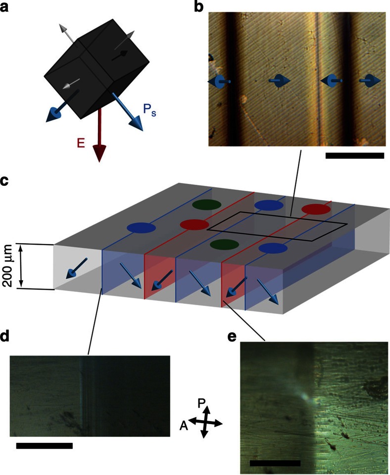
Figure 1. Charged domain walls in tetragonal BaTiO3.
(a) Poling of the crystal in a [110]c-like direction (red arrow) allows two equally preferred ferroelectric domain states (blue arrows) out of the six permitted (blue and grey arrows). When the frustrated poling is applied during a slow paraelectric-ferroelectric PT, tail-to-tail (b–d) and head-to-head (b,c,e) domain walls are formed. (b) Top view micrograph with light transmitted through the sample in the [110]c direction. Scale bar, 200 μm. (c) Out-of-scale cartoon illustrates a 200 μm thick (110)c sample with 5 × 5 mm2 top surface covered with 200 μm diameter and 400 μm period electrodes. The domain walls are irregularly distributed with period from 100 to 300 μm. (d,e) Side view micrographs with light transmitted in the [001]c direction show the tail-to-tail domain walls (scale bar, 100 μm) and head-to-head domain wall (scale bar, 25 μm), respectively. P denotes polarization of incident light and A polarization filter on transmitted light.

