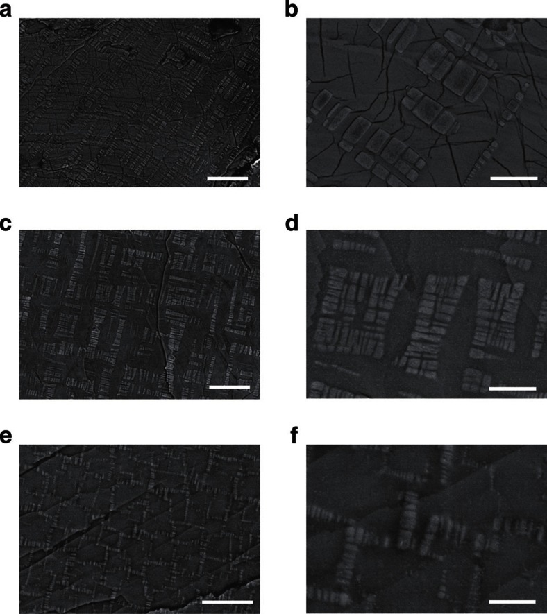
Figure 3. Back-scattered electron images of SEM measurements on the cleaved surface of three typical samples.
(a,b) The topography of the cleaved surface of the sample SFC. It is clear that the sample separates into two kinds of regions: the domains with brighter colour and rectangular shape, which are buried in the background of a darker region. Some cracks can be found in the background of the sample. The domains are widely separated. (a) Scale bar, 10 μm, (b) scale bar, 2 μm. (c,d) The topography of the cleaved surface of the sample S250. The domains with brighter colour in the sample of SFC further crack into many smaller domains, but are still far apart from each other. (c) Scale bar, 10 μm, (d) scale bar, 2 μm. (e,f) The SEM image of the sample S350. One can see that the domains become very small and well connected and form some networks which look like the spider-web. (e) Scale bar, 5 μm, (f) scale bar, 1 μm. The measurements were done with the voltage of 10 kV.

