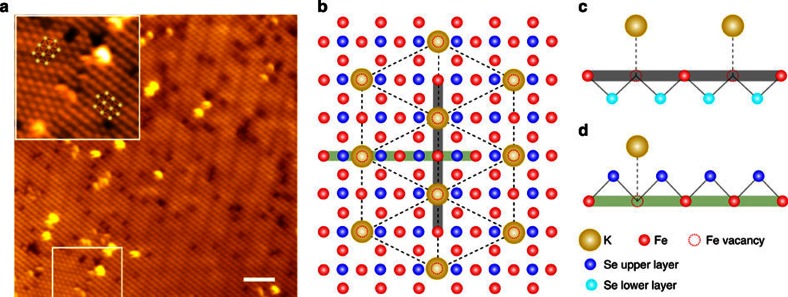
Figure 6. Atomically resolved topography and the sketch of the 1/8 Fe-vacancy  structure.
(a) The measured STM image on the [001] surface of the sample SFC with the proposed 1/8 Fe-vacancy  structure. The bias voltage and tunnelling current during the measurements are fixed at 4.2 V and 50 pA, respectively. The image on the upper-left corner is an enlarged view of the region enclosed by the frame on the bottom. In the inset, we use the white circles to represent the atoms of K. On the surface there are mainly two domains with different orientations, but they have the same structure, that is the
  parallelogram block. Scale bar, 5 nm. (b) Sketch of the K, Fe and Se atoms with the Fe vacancies in the beneath layer. The big yellow circles and hollow red circles with dashed-outlines represent the K atoms and the Fe vacancies, respectively. In our proposal they have the same
  parallelogram structure. (c,d) The partial structure constructed by the K, Fe and Se atoms when K resides just above the Fe vacancy, by crossing the two cuts along the traces highlighted by the thick grey and light-green lines in (b).

