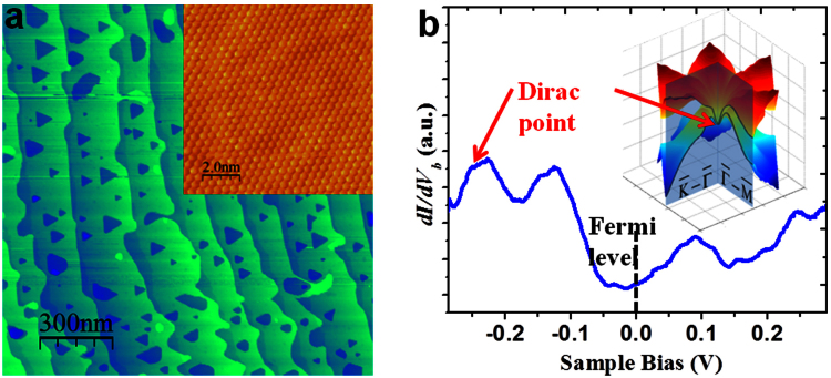
Figure 1. Atomic and electronic structures on Sb(111).
(a) STM image of 30 BL Sb(111) film grown on Si(111)-√3 × √3:Bi-β. Imaging conditions: Vb = −3 V, I = 50 pA. The inset shows the atomic-resolution image of Sb(111) surface (Vb = 1 V, I = 250 pA). The period is about 4.31 Å. (b) dI/dVb spectrum taken on 30-BL Sb(111) surface. The inset shows the schematic SS bands forming a Dirac point at  on Sb(111). By cutting the bands with vertical planes passing
  and
and  axes, the dispersions lines of SS along these high symmetry directions can be obtained.

