Figure 1.
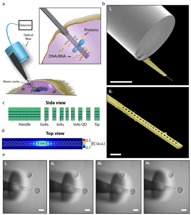
Photonic nanoprobe design and single cell interrogation. a, Schematic of photonic crystal nanobeam probe for single-cell investigation. The nanobeam cavity extends from a larger semiconductor template which is mounted on the side edge of a multimode optical fiber. The inset corresponds to the box in the main figure depicting potential sensing modalities of the cavity such as label-free protein or DNA/RNA detection. b, Angled scanning electron microscope (SEM) pictures of a typical fabricated device (in false-color). The ripple on the fiber facet is a small fracture from the fiber cleaver. A close-up of the beam portion is shown in b(ii). Some light debris from the sputter coating is also visible. The striations on the side of the beam are the three wetting layers of the self-assembled quantum dots. c, Schematic of the MBE material stack. The background material is GaAs and the quantum dots (shown as triangles) are InAs inside an InAs wetting layer. d, Finite-difference time domain simulation picture of the electric field magnitude of the fundamental cavity mode for this photonic structure. e, Sequence of bright-field images of a nanocavity probe penetrating a single PC3 cell, viewed from above. The probe is first positioned outside the cell with the membrane flexed and flush against the petri dish substrate. It is then maneuvered into the side of the cell and finally retracted. The optical fiber, which is positioned higher than the membrane is seen defocused in the pictures. Scale bars: 50 μm (b(i)), 1 μm (b(ii)), 20 μm (e).

