Figure 2.
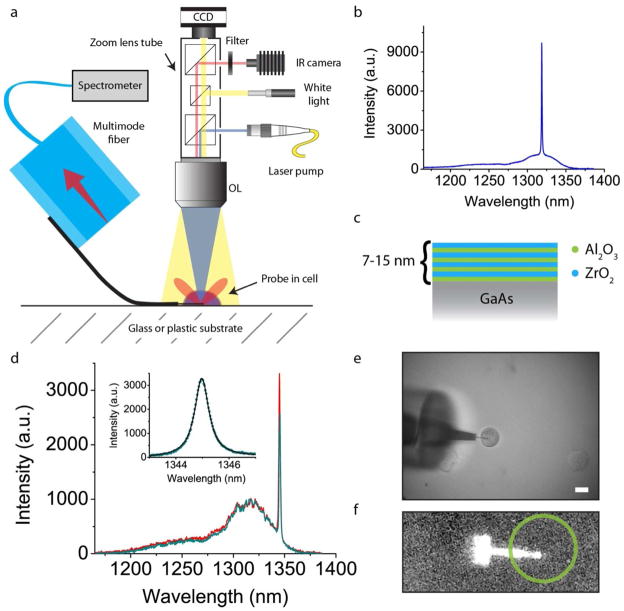
Optical characterization of photonic crystal cavities inside single cells. a, Diagram of the optical setup used in the experiment. A three-axis micromanipulator positions the probe such that the GaAs membrane (shown in black) flexes and rests against the substrate. A zoom lens tube contains beam splitters for laser pump and white light illumination, as well as image capture. OL is objective lens. Not shown is the liquid level, which submerges the optical fiber but does not reach the objective lens. b, PL spectrum of a single nanoprobe cavity measured in air. The QD emission uncoupled to the cavity is the small background spreading from 1,150 nm to 1,350 nm and the cavity mode is the sharp peak at 1,319 nm. c, Illustration of the alumina/zirconia nanolaminate used to coat the entire device, protecting it from photo-induced oxidation. Stacks alternated between 1 nm and 2 nm per layer thicknesses, and total stack thicknesses of 7–15 nm. d, PL spectrum of the same cavity from b now in a cell (teal) and its surrounding medium (red). There is negligible wavelength difference between the two spectra; however the collection intensity inside the cell (teal) is slightly lower, likely due to scattering from the plasma membrane. Inset shows a close-up of the cavity mode which has a Q-factor of 2,200. e, Corresponding white light image of the probe and cell for which data in d were taken. f, Corresponding IR image of the probe’s QD emission and a circular outline of the approximate cell location. Scale bar, 20 μm.

