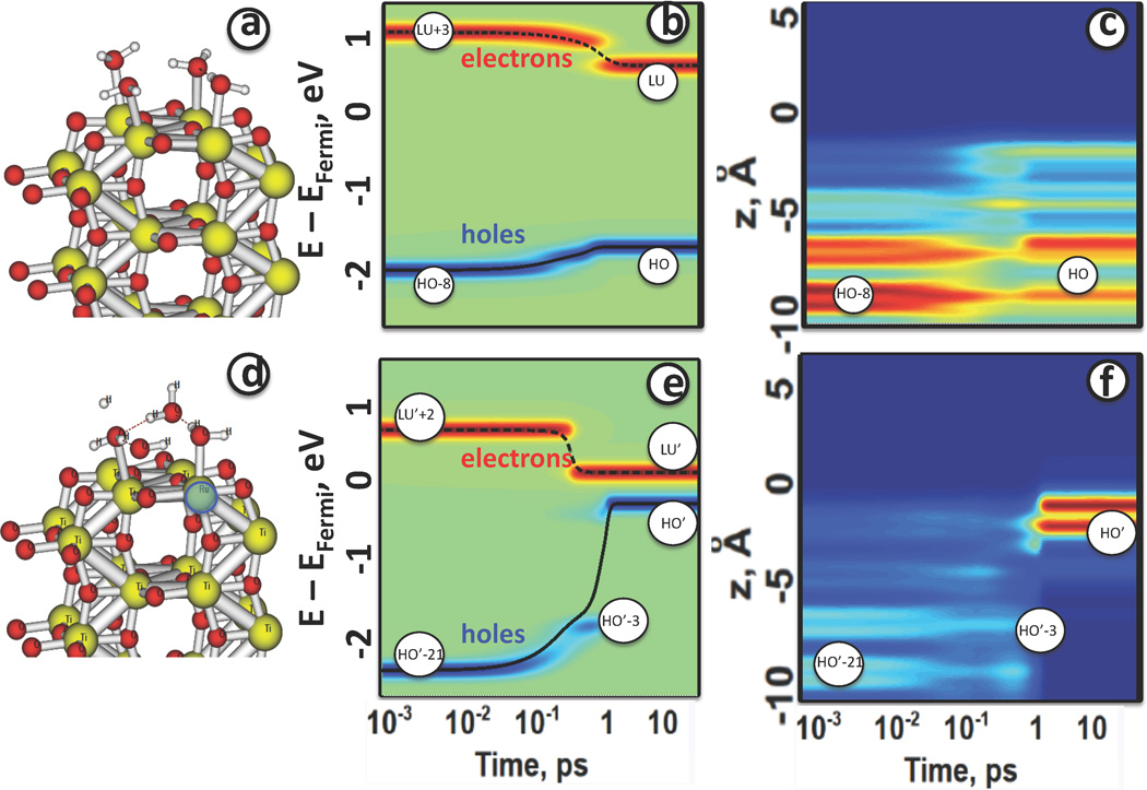
Figure 5.
a, d. Atomic models of thin semiconductor films with and without metal adsorbate. a: Ti32O64 × 8H2O; d: Ti30Ru2O64 × 8H2O. All models contain eight monoatomic layers, with 12 atoms each. The vertical axis z is perpendicular to the surface and is positive above the surface. Periodic boundary conditions are implied along x and y directions. Dangling surface bonds are compensated by water molecules. b, e. Isocontours of the population Δn(a,b)(ε, t) giving the dynamics of similar photoexcitations calculated for the silicon surface with and without surface adsorbed silver cluster. Here, red, green, and blue colored areas label the distribution Δn(a,b)(ε, t) in Eq. 16 for gain, no-change, and loss, respectively, in comparison with the equilibrium distribution; red areas can be understood as relating to electrons, and blue ones to holes. c, f. Spatial distributions as functions of time from Eq. 17. Colors from blue to red symbolize charge density value from 0 to 1. The figure presents the time evolution of electron density distribution in the normal direction to the surface for a silicon surface with and without an adsorbed silver cluster.

