Abstract
Colloidal quantum dot photovoltaics combine low-cost solution processing with quantum size-effect tuning to match absorption to the solar spectrum. Rapid advances have led to certified solar power conversion efficiencies of over 7%. Nevertheless, these devices remain held back by a compromise in the choice of quantum dot film thickness, balancing on the one hand the need to maximize photon absorption, mandating a thicker film, and, on the other, the need for efficient carrier extraction, a consideration that limits film thickness. Here we report an architecture that breaks this compromise by folding the path of light propagating in the colloidal quantum dot solid. Using this method, we achieve a substantial increase in short-circuit current, ultimately leading to improved power conversion efficiency.
Solution-processed solar cells offer the promise of low cost, large-area processing, and, prospectively, high solar power conversion efficiencies1,2,3,4. Colloidal quantum dots (CQDs) have attracted interest as photovoltaic light harvesters because, in addition to being processed from the solution phase, their bandgap can be tuned via synthetic control over nanoparticle size to optimize their spectral properties in the absorption of sunlight5,6,7,8.
Unfortunately, standing in the way of higher solar power efficiency is the fact that CQD materials today exhibit limited transport lengths9,10,11 compared to traditional, high-temperature-processed bulk semiconductors.
There exists therefore an urgent need to enhance absorption in a given thickness of CQD solid. Optical enhancements of absorption in ultrathin film semiconductor photovoltaics offer avenues to overcoming limited electronic transport in these materials. Progress has recently been made in this direction by engineering both the geometric12,13,14,15 and electronic landscapes16 in CQD devices, as well by improving the electrical back contacts at the semiconductor/metal interface17,18. Plasmonic absorption enhancements were recently shown19, and multijunction architectures offer a broadband approach to increasing solar cell performance20,21.
Results
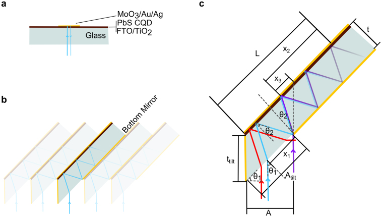
In the present work, we sought to increase the interaction of light with the absorbing CQD medium by passing light through the CQD layer multiple times. Multi-pass optical management shemes have been shown to be effective in crystalline silicon22,23,24 and dye-sensitized solar cells25. We would fold the light path in order to propagate light through the active layer more than the typical two normal-incidence passes. Figure 1a shows a flat depleted heterojunction3 device taking advantage of only two passes of light while a folded-light-path (FLP) device (Figure 1b) can take advantage of 6 passes, effectively absorbing all photons having energy greater than the CQD bandgap. Figure 1c illustrates the geometric constraints to achieving a periodically repeating structure. Equations relating angles θ1, θ2 and lengths x1, x2, x3, A, Atilt, L, t and ttilt can be found in SI 1.
Figure 1. Configuration and geometric considerations of FLP CQD solar cells.
(a) Conventional double-pass CQD solar cell. (b) Periodic arrangement of FLP CQD solar cell which takes advantage of multiple passes. (c) Geometric considerations for periodicity and multipass absorption. More details can be found in section SI 1.
We sought to assess quantitatively the extent to which the FLP strategy could enhance absorption, hence current. We began by exploring the spectral behaviour in the case of a 45° tilt angle. We show in Figure 2a the percentage contribution of each sequential pass in both the flat and the FLP architectures. Whereas only first and second passes can be considered in the flat case (grey and black dashed lines, respectively), we considered up to six full passes in the FLP case, wherein the length of each pass is scaled up by a factor of  .
.
Figure 2. Theoretical contributions of multiple passes on JSC.
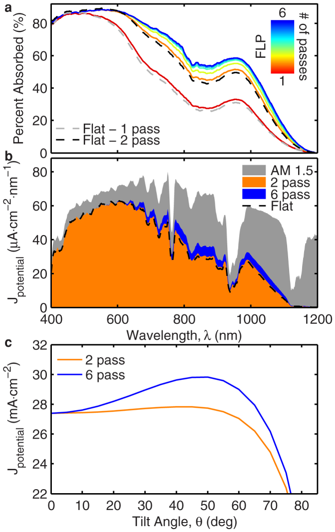
(a) Absorption contribution of the first two passes (grey and black dashed lines) of a flat DH CQD device and of the first six passes (colored lines) of a FLP DH CQD device. (b) Spectral current contribution of the first two passes and subsequent four passes of a FLP DH CQD device. The two-pass flat contribution is shown as dashed black curve. Grey area represents the AM 1.5 spectrum. (c) Tilting angle impact on total potential output current considering two passes (orange curve) and six passes (blue curve).
The contribution of the additional passes through the CQD layer translates into added photon current through spectral multiplication with the AM 1.5 solar photon fluence spectrum26 (Figure 2b, blue region versus orange region). We then proceeded to explore the impact of different choices of tilt angle. Figure 2c compares the two pass and six pass total achievable current as a function of tilting angle. The optimal calculated angle is approximately 50°, yielding a net potential short-circuit current density (JSC) enhancement of 3 mA·cm−2.
We fabricated devices where the CQD materials were synthesized and applied using the highest-photovoltaic-performance previously-published chemistry and materials processing8. For both the conventional flat device and the FLP device, the electron-accepting TiO2 layer was deposited by RC magnetron sputtering27. Masks were developed to accommodate the evaporation of the various metallic mirrors and electronic contacts (SI 2) for the FLP device. Briefly, edge mirrors of titanium, gold and silver were deposited, followed by titania on the fluorine-doped tin oxide (FTO) plane. Following an aqueous titanium chloride treatment and thermal annealing, we deposited a back mirror consisting of gold and silver. The CQD layer was then deposited in a layer-by-layer fashion using a solid state mercaptopropionic acid (MPA) treatment. Finally an elongated top contact/mirror consisting of molybdenum trioxide, gold and silver was deposited. Controls employed conventional contacts as described previously8. For more information, see methods.
The absorption characteristics of the flat and FLP devices were then explored. First, to look for qualitative evidence of multipass, we provide in Figure 3b (inset) a photograph of a sample illuminated through its aperture at a 45° tilt, leading to internal reflections and visual indication of at least six total passes through the film. This picture shows passes 1, 3 and 5 seen through the top of the device. Note that the active area of the device is defined by the light aperture, not the contact area28.
Figure 3. Absorption and external quantum efficiency of FLP devices.
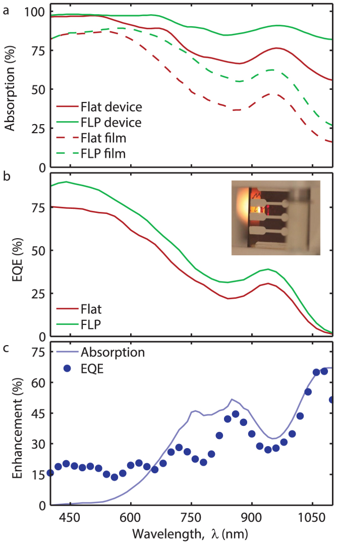
(a) Device (solid lines) and CQD film (dashed lines) absorption curves for flat (red) and FLP (green) samples. (b) External quantum efficiency of flat and FLP devices. (b – inset) Photograph of a tilted sample illuminated through the device aperture at 45° with a thin strip of white light demonstrating the capturing of multiple passes of light – in this case the third and fifth passes can be clearly observed. For photovoltaic measurements, the light aperture defined the active area dimensions28. (c) Absorption and EQE enhancement of a FLP device as compared to a flat device. Internal quantum efficiency curves can be found in section SI 3.
The absorption spectra of Figure 3a include both the total device absorption – including the glass, FTO and TiO2 layers – for the normal and 45° angled case; and also the absorption contribution of the CQD film alone. The measured absorbance includes effects from both the desired quantum dot film absorption, and also the undesired substrate and electrode absorption. The external quantum efficiency (EQE, Figure 3b) of the device, on the other hand, features only the benefits of the increase in quantum dot film absorption. In the infrared spectral range, where double-pass absorption is the lowest, the measured FLP case improvement is the greatest, and the enhanced absorption and EQE follow one another most closely. In the visible spectral range, the benefits of the FLP are accrued in fact in the first pass (i.e. it is not multipass/folding, but only tilting, that benefits EQE): absorption occurs closer to the front charge-separating interface, leading not to higher absorption, but to higher internal quantum efficiency in the tilted case. Convolving these EQE curves with the AM 1.5 solar spectrum and integrating generates expected JSC values of 25 mA·cm−2 to 21 mA·cm−2 in the FLP and flat devices, respectively.
To evaluate the impact on solar power conversion efficiency, we now consider as well the implications on voltage of the FLP architecture. Collecting current from the multipass device necessitates an increase in electrode area per sun-facing area of solar cell. Thus, in the equation for open-circuit voltage (VOC) as a function of short-circuit current (ISC), dark saturation current (I0) and Temperature (T)29
were k is the Boltzmann constant and q is the elementary charge, I0 is increased by the area of the FLP electrode.
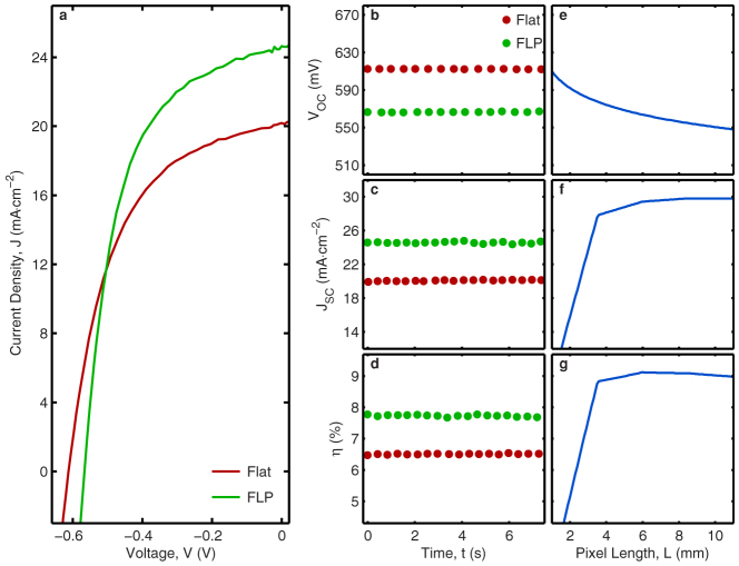
In our best FLP cells, our typical contact strip area was over 7 times larger than the aperture area due to geometric considerations, yielding an expected drop in VOC from our typical flat control of 0.61 V to 0.56 V (i.e. a loss of  as predicted in equation 1). The 15% expected improvement in JSC exceeds this 8% loss in VOC.
Experimentally, the FLP devices exhibited an enhanced current compared to planar controls of 24.6 mA·cm−2 versus 20.2 mA·cm−2 (Figure 4a,c), an increase of 4.4 mA·cm−2. The decrease in voltage (green compared to red markers in Figure 4b) also followed the predicted decrease (Figure 4e) from 0.61 V to 0.56 V. Overall, the power conversion efficiency, η, reported in Figure 4a and d, improved to AM1.5 solar η of 7.8 (the fill factor differences are negligible as they fall within the measurement error). For reference, Figure 4f and g illustrate the expected gain in current and η as a function of FLP electrode pixel strip length when considering purely optical light capture. Clearly notable is the 2 pass regime under ~3.25 mm, the 4 pass regime from ~3.25 mm to ~6 mm and the 6 pass regime from ~6 mm to ~8.75 mm. Subsequent passes were not considered as they contribute very little to additional JSC.
Figure 4. Measured and theoretical photovoltaic device performance.
(a) J-V characteristics of flat and tilted samples illustrating a ~4 mA·cm−2 enhancement in JSC and a ~0.05 V reduction in VOC. (b,c,d) Static VOC, JSC and η measurements, respectively, confirming a lack of rapid degradation and transient artefacts in flat and FLP device performance. (e,f,g) Theoretical implications of increased pixel strip length on VOC, JSC and η.
Discussion
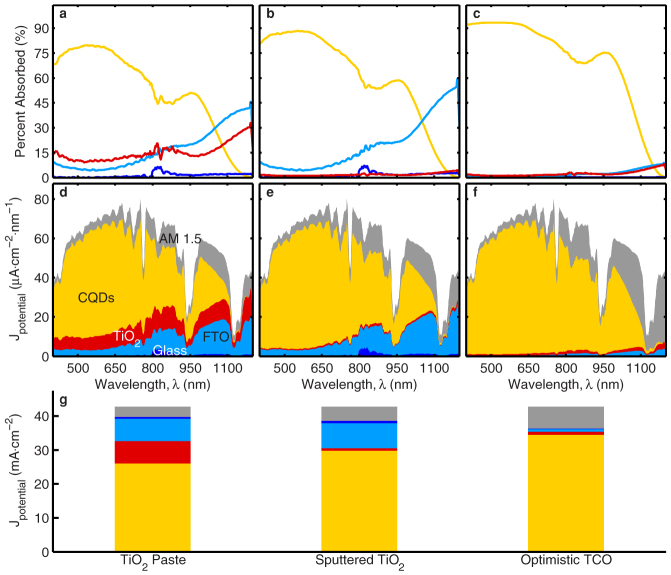
It is evident that any up-front absorption by the substrate and transparent contacts would compound unfavourably in a multipass context. To quantify this, we turned to the same model employed in Figure 2 while accounting for the glass, FTO and TiO2 layers of our typical depleted heterojunction devices. The electron-accepting TiO2 is ~500 nm thick and is formed from a colloidal paste. Figure 5a, d and g-left highlight the contribution of each of these layers, highlighting the impact of each in a 45° tilted FLP context. The thick TiO2 layer alone absorbs the photon equivalent of 6 mA·cm−2 of short-circuit current (red bar, Figure 5g), leaving the CQD layer with a best-case 26 mA·cm−2 JSC (yellow bar, Figure 5g). By employing a thinner, sputtered TiO2 layer (Figure 5b, e and g-middle), the FLP device improves its best-case JSCto 30 mA·cm−2. This is still far from the theoretical ideal 1.3 eV bandgap maximum of 36 mA·cm−2 30. To further illustrate the importance of all layers in the FLP stack, we also modeled the best-case scenarios for all layers in the stack, including thinner glass, highly transparent indium tin oxide (ITO), sputtered TiO2 as well as a perfect reflector at the top contact over all wavelengths of interest (Figure 5c, f and g-right). In this case, only Fresnel reflections at the front surface of the cell and the absorption coefficients of the CQD layer itself limit absorption. Through this analysis, it is possible to achieve over 34 mA·cm−2 of JSC.
Figure 5. Absorption contributions of constituent solar cell layers.
(a,b,c) Percentage absorption contribution and (d,e,f) spectral JSC contribution of glass (navy), FTO (blue), TiO2 (red) and CQDs (yellow) for FLP devices employing TiO2 paste (a,d), sputtered TiO2 (b,e) and an optimistic substrate/electrode combination (c,f). (g) Total absorbed photon equivalent JSC for all three cases.
This third condition, wherein the active layer has access to nearly all incident photons, suggests a further avenue to optimizing a solar cell employing a folded light path. The incoupling and trapping of light into the active layer is crucial to approaching complete absorption. It would be attractive to tailor the layers cladding the CQD material such that, following the first pass, light remained trapped within the CQD layer, wherein it would be waveguided and absorbed. In the absence of more strongly absorbing materials, folding the light path within the active layer of a solar cell remains a promising means to overcome the absorption versus extraction compromise.
Methods
Synthesis of PbS quantum dots and metal halide treatment
PbS quantum dots were synthesized according to a previously published method31. A solution-phase metal halide treatment (CdCl2) was then carried out following a previously published method8. Specifically, the metal halide precursor (1 mL of CdCl2) and tetradecylphosphonic acid (TDPA) were dissolved in oleylamine with 13.6:1 Cd:TDPA molar ratio. This mixture was introduced into the CQD reaction flask after the sulfur source injection during the slow cooling process. A 6:1 Pb:Cd molar ratio was adopted during the synthesis. At 30–35°C, the nanocrystals were isolated by the addition of 60 mL of acetone then subjected to centrifugation. The nanocrystals were then purified by dispersion in toluene and re-precipitation with a mixture of acetone/methanol (1:1 volume ratio), then re-dissolved in anhydrous toluene. The solution was further washed with methanol two more times before finally dispersing it in octane at a concentration of 50 mg/mL.
Substrate preparation
Cleaned FTO-coated glass substrates (Pilkington, TEC 15) with a 45° cut edge were employed in this study. We first deposited the edge mirror by e-beam evaporation of 5 nm of Ti at 1 Å/s followed by e-beam evaporation of 50 nm of Au at 1.5 Å/s followed by 100 nm of thermally evaporated Ag at 2 Å/s. 50 nm TiO2 (Kurt J. Lesker) was deposited to cover the substrate and its mirrored edge by RC magnetron sputtering at room temperature under Ar at 5 mTorr at a rate of 0.20 Å/s. Both deposition systems were Angstrom Engineering Åmod deposition systems located in an Innovative Technology nitrogen filled glovebox. The substrates were then treated with a 120 mm TiCl4 solution at 70°C for 30 min followed by a rinse with deionized water and annealing step on a hot plate at 520°C for 45 min in air ambient. The deposition of the bottom mirror was lastly done by e-beam evaporation of 50 nm of Au at 1.5 Å/s followed by 100 nm of thermally evaporated Ag at 2 Å/s.
Device fabrication
PbS CQD films were deposited using a layer-by-layer spin-coating process under an ambient atmosphere. For each layer, the CQD solution (50 mg/mL in octane) was deposited on the substrate and spin-cast at 2500 RPM for 10 s. Solid-state ligand exchange was performed by flooding the surface with 1% v:v MPA in methanol for 3 s before spin-coating dry at 2500 RPM for 10 s. Two rinses with methanol were used to remove unbound ligands. Each device consisted of 10 layers. The top contacts were finally deposited and consisted of 10 nm thermally evaporated MoO3 deposited at a rate of 0.2 Å/s, followed by e-beam deposition of 50 nm of Au deposited at 1.5 Å/s, and finally 120 nm of thermally evaporated Ag deposited at 2.0 Å/s.
AM 1.5 photovoltaic performance characterization
Current–voltage data were measured using a Keithley 2400 source meter. The solar spectrum at AM1.5 was simulated to within class A specifications (less than 25% spectral mismatch) with a xenon lamp and filters (ScienceTech; measured intensity of 100 mW·cm−2). The source intensity was measured with a Melles-Griot broadband power meter through a horizontal rectangular 0.02 cm2 aperture. We used an aperture slightly smaller than the top electrode to avoid overestimating the photocurrent: the entire photon fluence passing through the aperture was counted as incident on the device for all analyses of JSC and EQE28. The spectral mismatch of the system was characterized using a calibrated reference solar cell (Newport). The total AM 1.5 spectral mismatch - taking into account the simulator spectrum and the spectral responsivities of the test cell, reference cell, and broadband power meter - was re-measured periodically and found to be ~11%. This multiplicative factor, M = 0.89, was applied to the current density values of the J–V curve to most closely resemble true AM 1.5 performance32. The uncertainty of the current–voltage measurements was estimated to be ±7%.
EQE measurements
External quantum efficiency measurements were obtained by applying chopped (220 kHz) monochromatic illumination (400 W xenon lamp through a monochromator with order-sorting filters) collimated and cofocused with a 1 Sun intensity white-light source on the device of interest. The power was measured with calibrated Newport 818-UV and Newport 818-IR power meters. The response from the chopped signal was measured using a Stanford Research Systems lock-in amplifier at short-circuit conditions. The uncertainty in the EQE measurements was estimated to be ±8%.
Absorption measurements
Absorption spectroscopy was carried out using a Cary 500 UV-vis-IR Scan photospectrometer with an attached integrating sphere. The FLP devices were angled at 45° to mimic absorption in a tilted context.
Author Contributions
G.I.K. and S.H. conceived of the project and undertook initial experiments. G.I.K., I.J.K. and C.T.O.W. designed, fabricated, characterized and optimized devices. A.J.L. and C.T.O.W. optimized the electrodes. I.J.K. developed the optical model. S.M.T. aided in the design of experiments project coordination. I.J.K. and E.H.S. wrote the manuscript. All authors edited and reviewed the manuscript.
Supplementary Material
Supplementary Information for Folded-Light-Path Colloidal Quantum Dot Solar Cells
Acknowledgments
This publication is based on work in part supported by Award No. KUS-11-009-21, made by King Abdullah University of Science and Technology (KAUST). We thank Angstrom Engineering and Innovative Technologies for useful discussions regarding material deposition methods and control of glovebox environment, respectively. G.I.K. acknowledges NSERC support in the form of Alexander Graham Bell Canada Graduate Scholarship. The authors acknowledge the International Cooperation of the Korea Institute of Energy Technology Evaluation and Planning (KETEP) grant funded by the Korea government Ministry of Knowledge Economy (2012T100100740). The authors would also like to acknowledge the technical assistance and scientific guidance of E. Palmiano, L. Levina, R. Wolowiec and D. Kopilovic.
References
- O'Regan B. & Gratzel M. A low-cost, high-efficiency solar cell based on dye-sensitized colloidal TiO2 films. Nature 353, 737–740 (1991). [Google Scholar]
- Shaheen S. E. et al. 2.5% efficient organic plastic solar cells. Applied Physics Letters 78, 841–843 (2001). [Google Scholar]
- Pattantyus-Abraham A. G. et al. Depleted-Heterojunction Colloidal Quantum Dot Solar Cells. ACS Nano. 4, 3374–3380 (2010). [DOI] [PubMed]
- Todorov T. K., Reuter K. B. & Mitzi D. B. High-Efficiency Solar Cell with Earth-Abundant Liquid-Processed Absorber. Advanced Materials 22, E156–E159 (2010). [DOI] [PubMed] [Google Scholar]
- Luther J. M. et al. Schottky Solar Cells Based on Colloidal Nanocrystal Films. Nano Lett. 8, 3488–3492 (2008). [DOI] [PubMed] [Google Scholar]
- Luther J. M. et al. Stability Assessment on a 3% Bilayer PbS/ZnO Quantum Dot Heterojunction Solar Cell. Advanced Materials 22, 3704–3707 (2010). [DOI] [PubMed] [Google Scholar]
- Ma W. et al. Photovoltaic Performance of Ultrasmall PbSe Quantum Dots. ACS Nano 5, 8140–8147 (2011). [DOI] [PubMed] [Google Scholar]
- Ip A. H. et al. Hybrid passivated colloidal quantum dot solids. Nature Nanotechnology 7, 577–582 (2012). [DOI] [PubMed] [Google Scholar]
- Kramer I. J. & Sargent E. H. Colloidal Quantum Dot Photovoltaics: A Path Forward. ACS Nano 5, 8506–8514 (2011). [DOI] [PubMed] [Google Scholar]
- Zhitomirsky D. et al. Colloidal Quantum Dot Photovoltaics: The Effect of Polydispersity. Nano Letters 12, 1007–1012 (2012). [DOI] [PubMed] [Google Scholar]
- Guyot-Sionnest P. Electrical Transport in Colloidal Quantum Dot Films. J. Phys. Chem. Lett. 3, 1169–1175 (2012). [DOI] [PubMed] [Google Scholar]
- Leschkies K. S., Jacobs A. G., Norris D. J. & Aydil E. S. Nanowire-quantum-dot solar cells and the influence of nanowire length on the charge collection efficiency. Applied Physics Letters 95, 193103–193103–3 (2009). [Google Scholar]
- Barkhouse D. A. R. et al. Depleted Bulk Heterojunction Colloidal Quantum Dot Photovoltaics. Advanced Materials 23, 3134–3138 (2011). [DOI] [PubMed] [Google Scholar]
- Kramer I. J. et al. Ordered Nanopillar Structured Electrodes for Depleted Bulk Heterojunction Colloidal Quantum Dot Solar Cells. Advanced Materials 24, 2315–2319 (2012). [DOI] [PubMed] [Google Scholar]
- Lan X. et al. Self-Assembled, Nanowire Network Electrodes for Depleted Bulk Heterojunction Solar Cells. Advanced Materials 25, 1769–1773 (2013). [DOI] [PubMed] [Google Scholar]
- Kramer I. J., Levina L., Debnath R., Zhitomirsky D. & Sargent E. H. Solar Cells Using Quantum Funnels. Nano Lett. 11, 3701–3706 (2011). [DOI] [PubMed] [Google Scholar]
- Brown P. R. et al. Improved Current Extraction from ZnO/PbS Quantum Dot Heterojunction Photovoltaics Using a MoO3 Interfacial Layer. Nano Lett. 11, 2955–2961 (2011). [DOI] [PubMed] [Google Scholar]
- Gao J. et al. n-Type Transition Metal Oxide as a Hole Extraction Layer in PbS Quantum Dot Solar Cells. Nano Lett. 11, 3263–3266 (2011). [DOI] [PubMed] [Google Scholar]
- Paz-Soldan D. et al. Jointly Tuned Plasmonic–Excitonic Photovoltaics Using Nanoshells. Nano Lett. 13, 1502–1508 (2013). [DOI] [PubMed] [Google Scholar]
- Choi J. J. et al. Solution-Processed Nanocrystal Quantum Dot Tandem Solar Cells. Advanced Materials 23, 3144–3148 (2011). [DOI] [PubMed] [Google Scholar]
- Wang X. et al. Tandem colloidal quantum dot solar cells employing a graded recombination layer. Nature Photonics 5, 480–484 (2011). [Google Scholar]
- Sinton R. A., Kwark Y., Gan J. Y. & Swanson R. M. 27.5-percent silicon concentrator solar cells. IEEE Electron Device Letters 7, 567–569 (1986). [Google Scholar]
- Campbell P. & Green M. A. Light trapping properties of pyramidally textured surfaces. Journal of Applied Physics 62, 243–249 (1987). [Google Scholar]
- Heine C. & Morf R. H. Submicrometer gratings for solar energy applications. Appl. Opt. 34, 2476–2482 (1995). [DOI] [PubMed] [Google Scholar]
- Rühle S., Greenwald S., Koren E. & Zaban A. Optical Waveguide Enhanced Photovoltaics. Opt. Express 16, 21801–21806 (2008). [DOI] [PubMed] [Google Scholar]
- Standard Tables for Reference Solar Spectral Irradiances: Direct Normal and Hemispherical on 37° Tilted Surface. (2008). 10.1520/G0173-03R08.
- Koleilat G. I. et al. A Donor-Supply Electrode (DSE) for Colloidal Quantum Dot Photovoltaics. Nano Lett. 11, 5173–5178 (2011). [DOI] [PubMed] [Google Scholar]
- Snaith H. J. The perils of solar cell efficiency measurements. Nature Photonics 6, 337–340 (2012). [Google Scholar]
- Nelson J. The Physics of Solar Cells. (Imperial College Press, 2003). [Google Scholar]
- Henry C. H. Limiting efficiencies of ideal single and multiple energy gap terrestrial solar cells. Journal of Applied Physics 51, 4494–4500 (1980). [Google Scholar]
- Hines M. A. & Scholes, G. D. Colloidal PbS Nanocrystals with Size-Tunable Near-Infrared Emission: Observation of Post-Synthesis Self-Narrowing of the Particle Size Distribution. Advanced Materials 15, 1844–1849 (2003). [Google Scholar]
- Kroon J. M., Wienk M. M., Verhees W. J. H. & Hummelen J. C. Accurate efficiency determination and stability studies of conjugated polymer/fullerene solar cells. Thin Solid Films 403–404, 223–228 (2002). [Google Scholar]
Associated Data
This section collects any data citations, data availability statements, or supplementary materials included in this article.
Supplementary Materials
Supplementary Information for Folded-Light-Path Colloidal Quantum Dot Solar Cells


