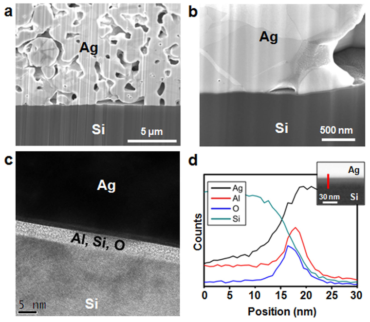
Figure 3. Cross section of Ag electrode.
SEM images obtained from the cross section of the contact between the Ag electrode and the Si wafer showing: (a) Sintered Ag electrode on the Si wafer; (b) Flat surface of the Ag particle in contact with the Si wafer surface. (c) Bright field TEM image obtained from the cross section of the contact between the Ag electrode and the Si wafer; (d) EDS line profile along the red line marked in the inset (dark field TEM image) showing enrichment of Al and O in the interface layer. The ultra-thin interface layer (~ 5 nm) between the Ag electrode and the Si wafer enables efficient carrier transfer through the interface by direct tunneling, thus finally results in the high cell efficiency of the solar cell.

