
Figure 2. Structural characterization.
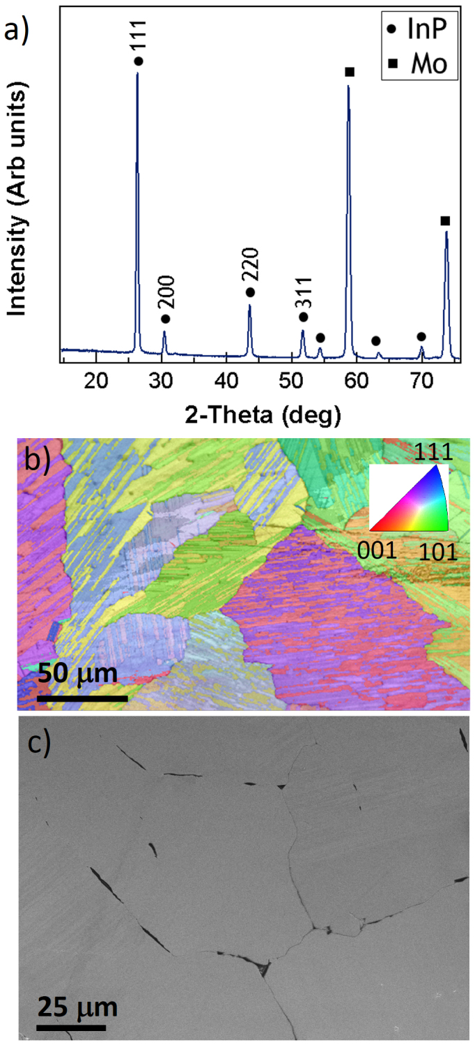
(a), XRD spectrum of an InP film grown at 750°C. (b), EBSD image of the backside of a peeled off TF-VLS InP film, indicating large grain sizes of ~10–100 μm. (c), Top-view SEM image of InP peeled off from Mo foil, partially etched in 1% HCl to highlight grain boundaries.