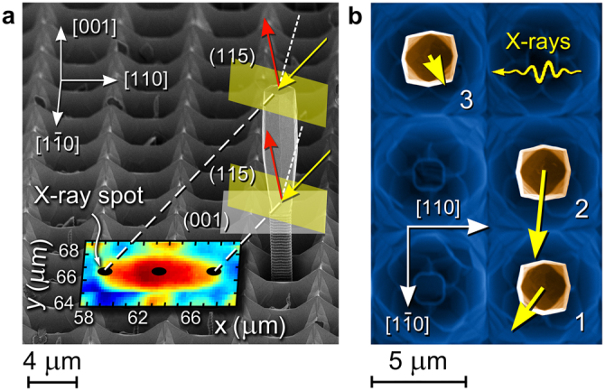
Figure 3. Probing the random net tilts of Ge crystals.

(a), Scattering geometry for the (115) Bragg reflection for an 8-μm-tall-Ge crystal on a patterned Si(001) wafer with 8-μm-tall and 2-μm-wide Si pillars, spaced by 4 μm. Neighbouring Ge crystals were removed. One (001) and two (115) planes are shown by transparent grey and green areas, respectively. The yellow arrows indicate the incident X-ray beams for two positions along the crystal height (bottom and top), and red arrows are the corresponding diffracted beams. The color map superimposed onto the perspective-view SEM micrograph represents the scattered intensity collected around the Ge(115) peak for an incidence angle of ω = 46.3° when the incident beam was moving along the length of the crystal. (b), Top-view SEM micrograph of three Ge crystals. The direction of incident X-rays is indicated (scattering geometry is similar to that shown in (a). The yellow thick arrows starting from the centre of each Ge crystal are the displacement vectors of the symmetry axes of the crystals from the [001] direction multiplied by 500 to enhance the visibility of local tilt.
