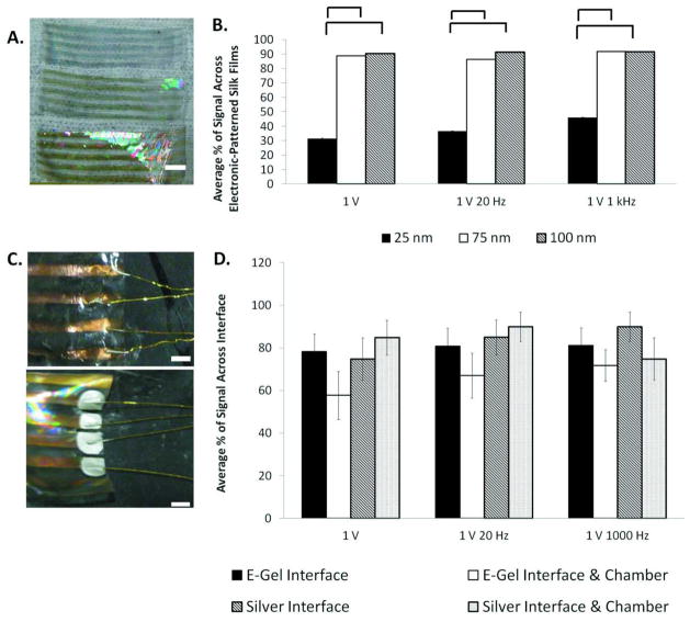
Figure 3. Conductivity Across Electronic Silk Films.
(a) Images of electrode thickness on silk films at 25 nm (top film), 75 nm (middle film), and 100 nm (bottom film). Scale bar is 10 mm. (b) Conductivity measurements across electronic films at 25 nm, 75 nm, and 100 nm thickness. Statistical significance between groups is marked by a bracket (p < 0.05). (c) (top) e-gel interface across silk films and (bottom) silver interface across silk films. Scale is 2 mm. (d) Conductivity across interface and chamber. Statistical significance between groups is marked by an asterisk (* p < 0.05).

