
Figure 5. Electronic Silk Film Modeling.
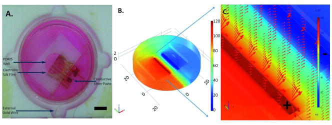
(a) Image of the modeled electronic silk film and chamber. Scale bar = 1 cm. (b) Maximum voltage applied to the chamber. Color bar is in mV. (c) Electric field strength and electric field direction is illustrated by the red arrows. Electrodes designated as anode and cathode are outlined and then marked by a positive and negative symbol, respectively.