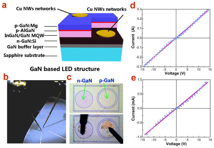
Figure 4.
(a) Schematic illustration of the GaN-based LED structure together with Cu NW TEs on n- and p-type areas; (b) photograph of the setup of EL measurement of LED devices on a probe station; (c) optical micrographs of an individual LED unit before and after imprint of Cu NW TEs; (d) and e) I-V characteristics of the contact of Cu NW TEs to n-GaN and p-GaN, respectively. The Ohmic contact behavior is obtained with optimized annealing condition.

