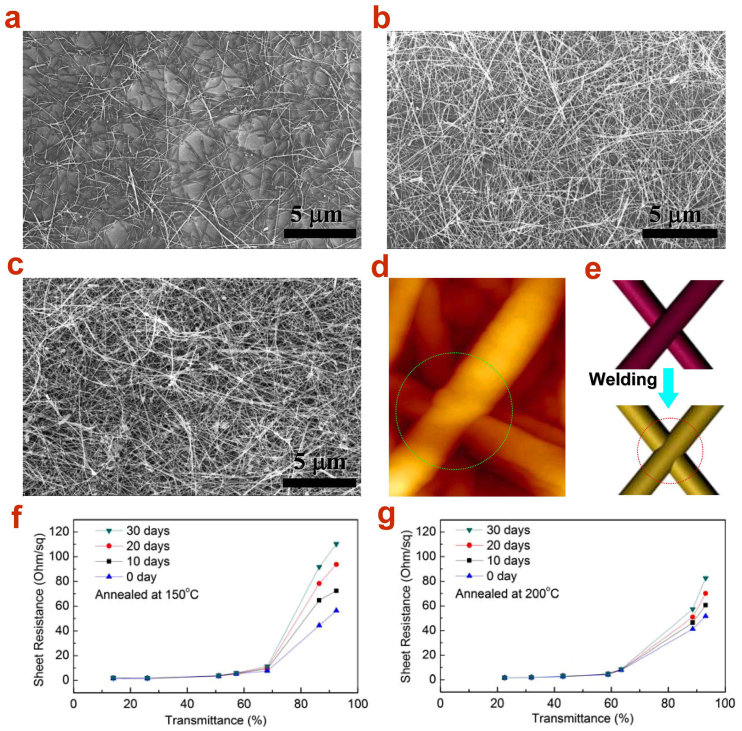
Figure 7.
(a–c) SEM images of the Cu NW TEs on glass substrates with a transmittance at 87%, 62.8% and 32.8%, respectively. (d) AFM image of Cu NW after annealing at 200°C for 1 h, where the welding point has been formed, and (e) schematic of the nanowelding between two NWs before and after annealing. (f) and (g) Transmittance vs. sheet resistance for the Cu NW TEs which were annealed at 150°C and 200°C, respectively, and exposed in air for 30 days. Annealing at 200°C can significantly improve the stability of Cu NW TEs.

