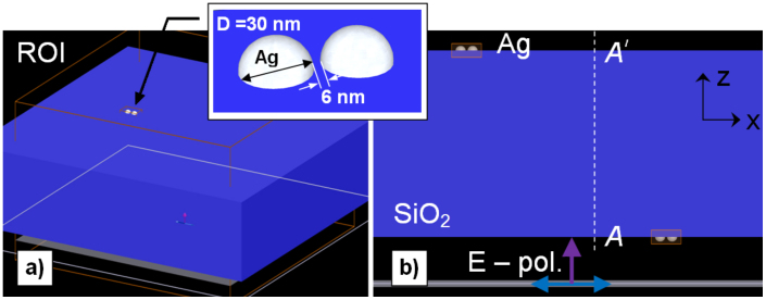
Figure 4. FDTD modeling domain (region of interest - ROI) comprising a silica slab of 1 μm thickness (in blue) and two pairs of hemispherical silver nanoparticles, positioned at 1 μm spacing on the near side (x-positive) and far side (x-negative) with respect to the x-polarized plane wave source (white square).
Projections are shown for (a) 3D perspective, (b) xz-plane. Inset in (a): a detail of the nanoparticle pair is shown, the sphere diameter is 30 nm, and the nanogap width is 6 nm. The A–A′ cross section was used to estimate the field distribution at the dielectric boundary.

