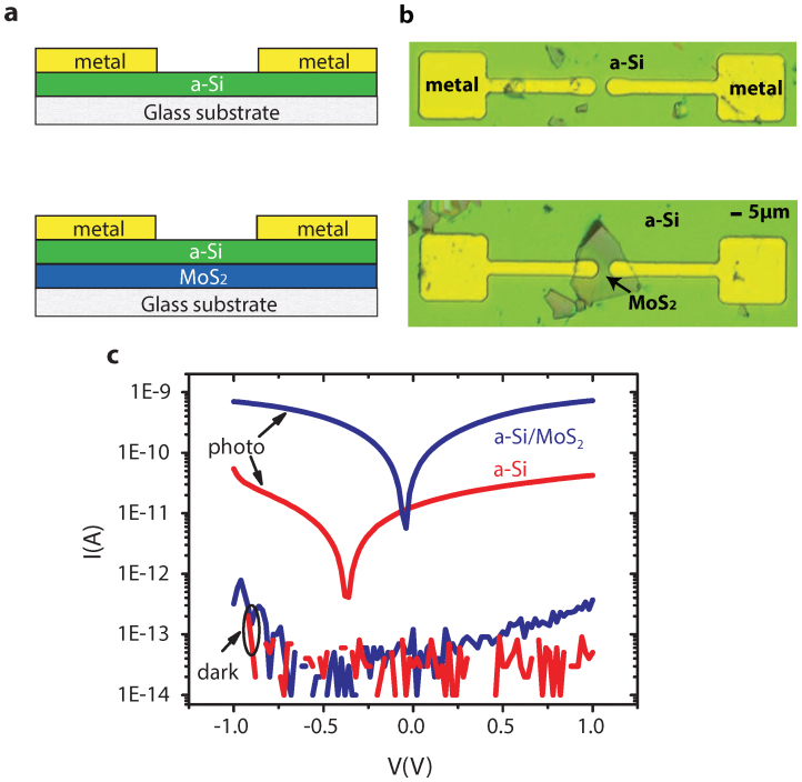
Figure 2.
(a) Schematic of cross sections of two metal-semiconductor-metal (MSM) photodetectors and (b) corresponding top view photomicrograph of devices. The length and width of devices is about 5 and 6 μm, respectively. (c) Measured dark and photo current-voltage (IV) characteristics. The semiconductor layer is 100 nm a-Si film (labeled as a-Si), and 60 nm MoS2 flake covered by 100 nm a-Si (labeled as a-Si/MoS2), see Supplementary Materials and Figure S1 for further details.

