Figure 6.
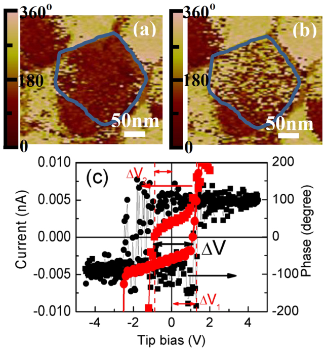
PFM images of ZnO nanoisland in vertical contrast at room temperature for (a) after process (2), and (b) after process (4). (c) PFM hysteresis phase loop (right axis) and further zoomed-in I–V characteristics (left axis). The overall electric fields in the ZnO nanoisland are opposite after process (2) and (4), respectively, which corresponds to the formation of C-AFM/ZnO Schottky diode and n-ZnO/Si substrate diode under these conditions. The smallest voltage window (ΔV) to induce phase change matches V1 (1.1 V) and V2 (−0.9 V) very well, which is a direct evidence of the need of reduce the built-in field to turn on each diode. These built-in fields correlate with the observed turn-on voltages.

