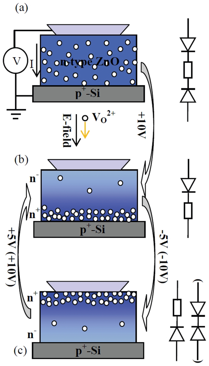
Figure 7. Schematic illustration of switching mechanism of C-AFM tip/ZnO nanoisand/Si substrate resistive memory to explain the observed threshold-like and self-rectifying bipolar switching behavior.
(a) The initial state, showing that the nanoisland system can be modeled as being composed of one Schottky diode consisting of the C-AFM tip and nanoisland and one p+-n diode consisting of the Si substrate and ZnO nanoisland connected back to back, in series with the semiconducting ZnO nanoisland with a resistor R. (b) Conversion of p+-Si/n-ZnO rectifying junction to p+-Si/n+-ZnO tunnel junction as a result of diffusion of the oxygen vacancies after a voltage sweep from 0 V to +10 V. In this case, the p+-Si/n+-ZnO tunnel junction can be treated as a resistance and there is only one rectifying junction in the loop. (c) C-AFM tip/ZnO Schottky junction converts to Ohmic junction or keeps as Schottky junction depending on the current compliance as a result of diffusion of oxygen vacancies after the voltage sweep from 0 to −5 V or −10 V. The Schottky junction can be treated as a resistor at current compliance of 10 nA because of current tunneling through the very thin barrier. Current self-rectifying resistive switching occurs when the Schottky diode can be treated as a rectifying diode rather than a resistor, as shown in the bracket in (c), in which tunneling current of 10 nA no longer represents LRS because of higher current value after the voltage sweeping from 0 to 10 V. At the same time, the p+-n+ tunneling diode between the substrate and ZnO nanoisland turns into a p+-n heterojunction. During the voltage sweep from 0 to 5 V or 10 V as indicated by an arrow pointing from (c) to (b), similar reaction occurs as in voltage sweep of 0 ~ −5 V or −10 V.

