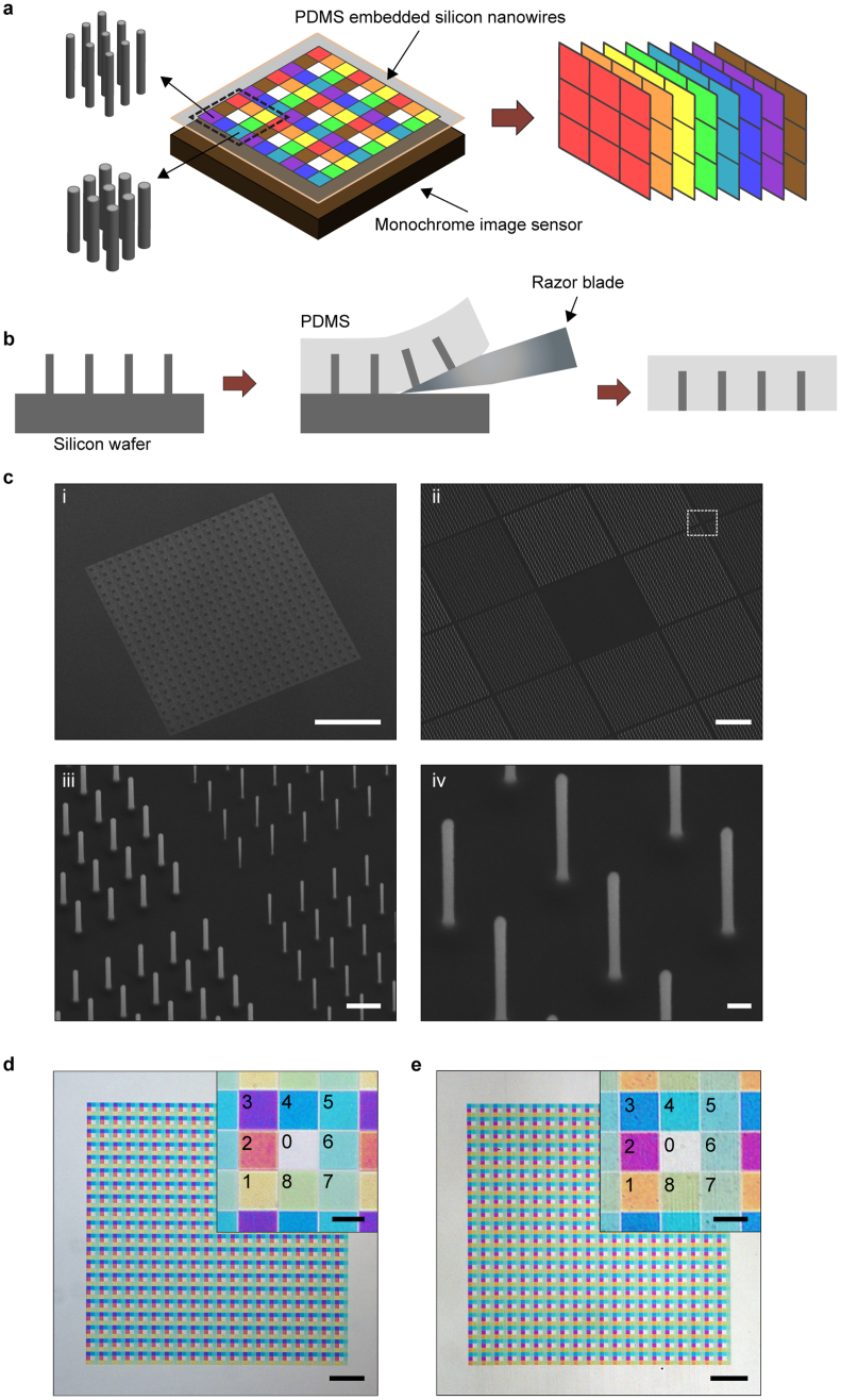
Figure 1.
Multispectral filter based on vertical Si nanowires (a) Concept schematic of multispectral imaging system. (b) Fabrication steps for multispectral filter. (c) SEM image of array of etched vertical silicon nanowires (30° tilted view). Array is composed of 20 × 20 unit cells. Each unit cell (75 × 75 μm) has eight different filters (each 23 × 23 μm), plus transparent region in its center. Each filter is composed of 24 × 24 nanowires and has an extent that corresponds to 4 × 4 pixels of the image sensor employed in our experiments. We intentionally choose the size of each filter to correspond to multiple image sensor pixels, rather than to a single pixel, to make it easier to align the device to the sensor chip. Scale bars i-iv are 500 μm, 10 μm, 1 μm and 200 nm. Nanowires with eight different radii (45 nm to 80 nm in 5 nm steps) are fabricated. Heights of all nanowires are 1.67 μm, and pitch is 1 μm. iii shows magnified view of boxed area of panel ii. Radii of nanowires are 45 nm, 50 nm, 70 nm and 75 nm (counter clockwise from upper right corner). iv shows nanowires with radii of 50 nm. (d) Reflection-mode optical microscope image of etched vertical silicon nanowire array on silicon substrate. Scale bars are 200 μm and 20 μm (inset). Inset shows magnified image of unit cell of array. Channels are numbered and contain nanowires with radii as follows. Channel 0:no nanowires, 1:45 nm, 2:50 nm, 3:55 nm, 4:60 nm, 5:65 nm, 6:70 nm, 7:75 nm, 8:80 nm. (e) Transmission-mode optical microscope image of PDMS-embedded vertical silicon nanowire array. Scale bars are 200 μm and 20 μm (inset).

