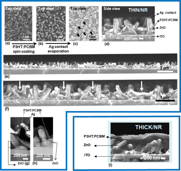
Figure 2.

SEM/STEM characterization. (a) Electrodeposited ZnO nanorod arrays, (b) arrays coated with a thin P3HT:PCBM highly conformal layer, (c) Ag contact evaporated on top of the P3HT:PCBM layer (Thin/NR cells) with arrows indicating a few spots where shadowing from the nanorods prevented Ag deposition, (d) cross-sectional image of a Thin/NR cell, (e, f) cross-sectional images of different areas of the Thin/NR cell, (g, h) STEM images of cross sections of Thin/NR samples and (i) cross-sectional image of a conventional hybrid cell (Thick/NR).
