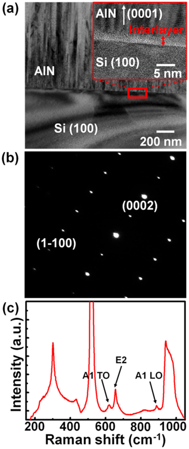
Figure 1. (a) Cross-sectional TEM image of the AlN thin films deposited on a Si(100) substrate.
The inset shows the high-resolution TEM image of the marked area in (a). (b) The electron-diffraction pattern of the AlN films. (c) Raman spectrum of a 1-μm-thick AlN on Si(100) deposited by reactive sputtering at 350°C.

