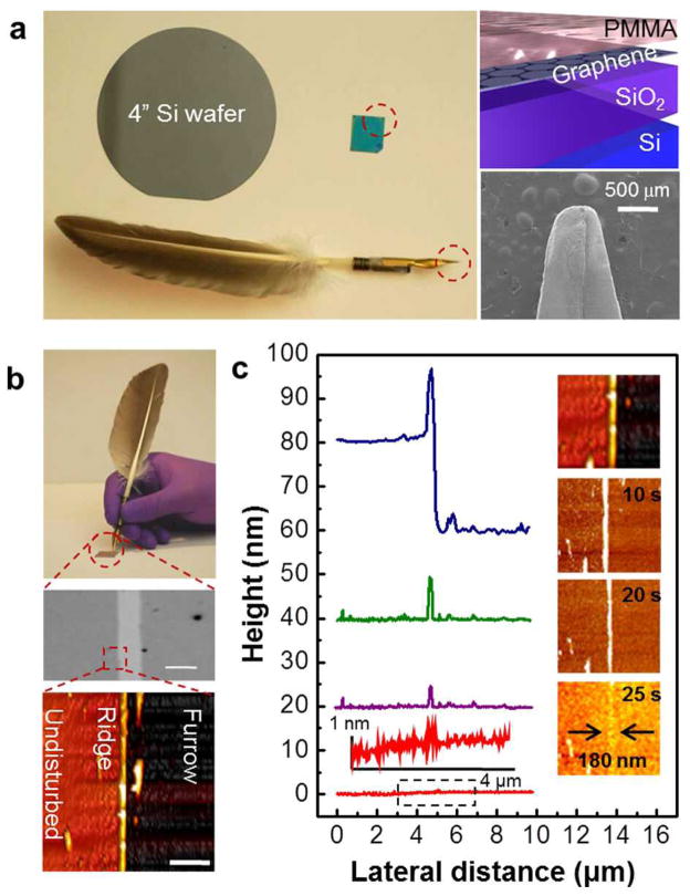
Figure 1.
a) Quill pen with a tip diameter of 500 μm shown with a 4″ Si wafer for scale. The pen is used to write a line on a Si wafer chip on which graphene has been deposited and coated with 25 nm film of poly (methyl methacrylate) PMMA. b) Writing a line on the surface (top panel) results in a clear furrow (middle panel, scale bar: 500 μm). Atomic force microscope (AFM) image of the edge of the furrow depicting the undisturbed region, the furrow, and the ridge between them (bottom panel, scale bar: 1μm). c) Height profiles and corresponding AFM images of time evolution (as-written, 10 s etching, 20 s total etching, and 25 s total etching) of the surface under an anisotropic reactive ion etching (RIE) process. AFM images are 2 μm in width.

