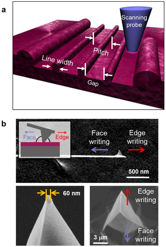
Figure 2.
a) Schematic illustration of writing with a scanning probe tip on a polymer surface. b) Scanning electron microscopy (SEM) images of a commercial Si AFM probe. Edge- and face-first writing directions are defined based on the direction of tip movement. The inset schematic illustrates the geometric difference between edge- and face-directed writing.

