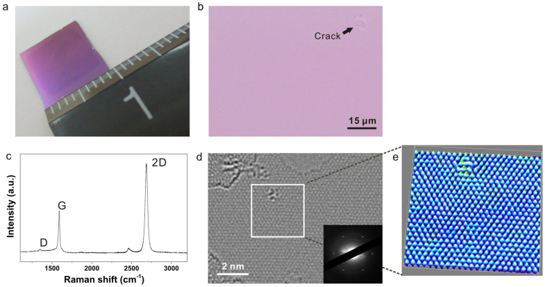
Figure 2. Graphene films transferred from Ga–W substrate.
(a) Graphene film transferred onto a SiO2/Si substrate. (b) Optical image of the transferred graphene on a SiO2/Si substrate. (c) Raman spectrum of the single-layer graphene. (d) HRTEM image and the selected-area electron diffraction pattern (inset) of the single-layer graphene. (e) A false 3D image originated from Fourier enhanced TEM micrograph of the marked area in Fig. 2d.

