Abstract
This paper reports the design, fabrication, and performance of miniature micromachined high frequency PMN-PT/epoxy 1-3 composite ultrasonic annular arrays. The PMN-PT single crystal 1-3 composites were made with micromachining techniques. The area of a single crystal pillar was 9 μm × 9 μm. The width of the kerf among pillars was ~ 5 μm and the kerfs were filled with a polymer. The composite thickness was 25 μm. A six-element annular transducer of equal element area of 0.2 mm2 with 16 μm kerf widths between annuli was produced. The aperture size the array transducer is about 1.5 mm in diameter. A novel electrical interconnection strategy for high density array elements was implemented. After the transducer was attached to the electric connection board and packaged, the array transducer was tested in a pulse/echo arrangement, whereby the center frequency, bandwidth, two-way insertion loss (IL), and cross talk between adjacent elements were measured for each annulus. The center frequency was 50 MHz and -6 dB bandwidth was 90%. The average insertion loss was 19.5 dB at 50 MHz and the crosstalk between adjacent elements was about -35 dB. The micromachining techniques described in this paper are promising for the fabrication of other types of high frequency transducers e.g. 1D and 2D arrays.
1. INTRODUCTION
Until recently most medical high-frequency (> 30 MHz) ultrasound imaging systems are based on single-element transducers, which are either unfocused or geometrically focused at a certain fixed depth. The fixed focus imposes limitations on lateral resolution and depth of field (DOF). Linear arrays and 2-dimensional (2-D) arrays are desired for their capabilities in beam steering, dynamic focusing, and higher image frame rate. At present, commercial high frequency array systems are not yet available at frequencies above 50 MHz mainly due to limitations in fabricating of hundreds or even thousands small-scale elements, electrical interconnections, and system development. However, annular array transducers for high frequency ultrasonic imaging can bridge the gap between single-element transducers and linear/2-D array transducers, which can be dynamically focused, yielding better image quality than fixed focus single-element transducers. Compared to linear/2-D arrays, annular arrays have fewer elements which simplify the fabrication and require less complex electrical systems. The drawback is that mechanical scanning is still needed. Several researchers have developed high frequency annular arrays. Brown et. al., [1], fabricated a kerfless array by patterning aluminum electrodes on a planar PZT-5H substrate. Ketterling et. al., [2] developed a 40-MHz annular array transducer using PVDF material whereas Gottlieb et. al., [3], used P(VDF-TrFE) film and a doubled sided flex circuit to fabricate a similar transducer. These piezoelectric polymer based kerfless arrays in general tend to have a low sensitivity due to its low clamped dielectric constant and kt values, which may be better suited for fabricating transducers at lower frequencies or with large aperture sizes. Kerfless PZT array suffers high cross talks between adjacent elements.
Piezoelectric composite materials have many attractive characteristics for ultrasonic transducer applications, especially for array transducers. PMN-PT/epoxy 1-3 composites offer a large number of design parameters, including the PMN-PT pillar dimension, epoxy selection, and volume fraction of PMN-PT, which can be easily tuned to optimize composite material performance for a certain application. Firstly, for 1-3 composite material, piezoelectric pillars may be embedded in soft epoxy matrices, thus minimizing lateral clamping between active piezoelectric elements. As a result, a higher electromechanical coupling coefficient for the composite can be obtained than that of the bulk material operating in a plate mode [4]. PMN-PT single crystals have the highest pillar mode piezoelectric properties (k33 over 0.90). Furthermore, this special structure can significantly decrease inter-element crosstalk, which is very critical for the high frequency array transducer with small elements. Secondly, with the addition of epoxy, the effective acoustic impedance of the composite is much lower (~18 MRayls) than that of single crystal PMN-PT (~ 30 MRayls). This facilitates better acoustic impedance matching between the transducer and human tissue, which results in improved energy transmitting and receiving. Thirdly, the shape and layout of piezoelectric pillars can be adjusted to avoid spurious resonances generated in periodic composites. As a result, wider bandwidths can be obtained; hence axial resolution can be improved.
The two greatest challenges in developing high frequency ultrasonic arrays are: 1) fabricating elements that are very small, and 2) the construction of an electrical interconnection system for array elements with narrow pitches. These problems also exist in the fabrication of high frequency annular arrays, although they are alleviated to a certain extent because of the comparatively smaller number of elements. Nevertheless new methodologies are required for the development of high frequency annular arrays. Fabrication of PMN-PT composite for high frequency arrays requires that the pillars/kerfs have very small dimensions. For example, at 70 MHz, the pillar size should be less than 10 μm. For the current study a kerf width of ~ 5 μm was selected. The traditional dicing-and-filling method [5, 6] and other precise machining methods, such as laser ablation [7], cannot accomplish the task. Based on interdigital pair bonding techniques [6], Chabok et. al., [8] developed a 35 MHz PZT 1-3 composite annular array transducer using dicing technology. Microfabrication techniques [9] and MEMS technologies [10] on the other hand offer an easier alternative for the production of PMN-PT composite materials and development of high frequency ultrasonic arrays. However, till now there are no such efforts in developing high frequency array transducers using micromachining techniques.
For high-frequency arrays, electrical connection to each element is preferentially made on the back side of the transducer, which simplifies the top surface topology. Current electric interconnection methods for array transducers include wire bonding [1], flex circuits [2], and multi-layer thick film circuits [11]. With the wire bonding method, fine metal wires must be bonded onto each element; this limits the utility of the process to larger number of elements. Flex circuits or multi-layer circuits are directly attached to the array elements to expand electrical connections. The backing material is then added on the circuits. They are widely used in low frequency array transducers. However, acoustic impedance mismatching between flex circuits and the backing material sometimes cannot be tolerated by high frequency ultrasound transducers. A better and often used approach for high-frequency transducer design is to directly attach the piezoelectric element to a conductive backing material [12]. Poor adhesion to the backing material and wire connection may cause long ringing in the pulse echo waveform, which has been observed by [10]. Thus, a better electrical connection method needs to be explored.
In this paper, a first attempt in utilizing micromachining and MEMS (Micro-Electro-Mechanical System) technologies to fabricate high-frequency ultrasonic annular array transducers is reported. PMN-PT/epoxy 1-3 composite was produced by micromachining processes, combining photolithography and dry etching techniques. A conductive backing material was directly attached to each array element and separated by an insulating mold. In addition, a new electric connection strategy was implemented that could be applied to many types of array transducers with fine elements and narrow pitches.
2. ARRAY DESIGN
A common design for annular arrays entails making the area of each element equal. The array discussed here had an aperture diameter of approximately 1.3 mm with six equal area (0.2 mm2) elements separated by 16-μm kerfs. The radius of the center circle element r1 was 250 μm. The outer radii of the other five annuli were calculated using the following equation:
| (1) |
where kerf represents the spacing between elements. The desired central frequency was 50 MHz. The kerf between elements was a constant value of 16 μm. The effective inner and outer radii for each element were listed in Table 1.
Table 1.
Geometry for annular array
| Element No. | Inner radius (μm) | Outer radius (μm) | Width (μm) |
|---|---|---|---|
| 1 | 0 | 250 | 250 |
| 2 | 266 | 365 | 99 |
| 3 | 381 | 456 | 75 |
| 4 | 472 | 534 | 62 |
| 5 | 550 | 604 | 54 |
| 6 | 620 | 668 | 48 |
PMN-PT/epoxy 1-3 composite with a PMN-PT volume fraction of about 50% was used. Composite piezoelectric materials have many advantages as mentioned above. However, there are lateral resonance modes between periodically placed pillars of the composite, which limit the highest working frequency of the material. In this work, a random layout of the pillars was used to avoid periodic arrangements. All pillars were laid out concentrically with no parallel edges, and the distance between each pillar was not exactly the same. This kind design restricted spurious resonance modes in the composite and at the same time improved bandwidth. The kerf width of the composites averaged about 6 μm and the dimension of the pillars was 9 μm by 9 μm.
To predict the performance of the annular array, a series of simulations using Field-II [13] and PiezoCAD (Sonic Concepts, Inc., Bothell, Washington) were carried out, which is similar to [14]. Table 2 summarized some key design parameters, material selection, and simulation results for the array transducer. With 8 μm-thick parylene as a matching layer and E-solder as the backing material, the central frequency of the array transducer was 51 MHz and the -6dB bandwidth 88%.
Table 2.
Design parameters, material selection, and simulation results of annular array
| Piezoelectric material | 50% volume fraction PMN-PT composite |
| Thickness | 25 μm |
| Number of elements | 6 |
| Area of each element | 0.25 mm2 |
| Matching layer | 8 μm parylene |
| Backing material | E-solder |
| Central frequency | 51 MHz |
| -6 dB Bandwidth | 88% |
| -6 dB pulse width | 16 ns |
3. ARRAY FABRICATION
3.1 PMN-PT 1-3 Composite and Transducer stack
In our current design, the PMN-PT/epoxy 1-3 composite was produced using microfabrication processes, combining photolithography and dry etching techniques. This has several advantages, such as batch processing, submicron machining precision, and low cost for mass production. Fig. 1 illustrates the process flow for PMN-PT/epoxy 1-3 composite fabrication.
Fig. 1.
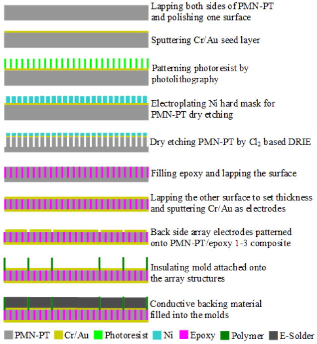
Schematic process flow for micromachining a PMN-PT/epoxy 1-3 composite annular array transducer with conductive backing material.
A single crystal PMN-PT plate (H. C. Materials, Bolingbrook, IL) with dimensions of 25 mm by 12 mm and 0.65 mm thickness was lapped on both surfaces down to a thickness of 0.5 mm and polished on one side. A thin layer of Cr/Au was sputtered onto the polished side as an electroplating seed layer. A 10 μm thick layer of positive photoresist was spin-coated onto the substrate and baked at an elevated temperature of 100 °C for 5 minutes. Then the sample was directly exposed using a DWL 66 Laser Writer (Heidelberg Instruments, Mikrotechnik GmbH, Germany). The sample was developed in an MF-CD-26 developer (Rohm and Haas Electronic Materials LLC, Marlborough, MA) for 10 minutes.
After O2 plasma descumming, the sample was dipped into a nickel electroplating bath to plate a layer of Ni as the hard mask for dry etching. The temperature of the bath was 45°C, the average current intensity 20 mA/cm2, and the final thickness of the plated nickel about 7 μm, which was enough to protect PMN-PT during dry etching to a depth of 30 μm. To obtain a high density nickel layer, a pulsed power supply (DuPR10-1-3, Dynatronix, Inc., Amery, Wisconsin) was used in the plating system. After electroplating, the photoresist was stripped off using acetone. The sample was then placed in a chlorine-based dry etching chamber for etching. The etching rate was ~160 nm/min, and selectivity of nickel to PMN-PT was about 1:6. The profile angle was about 85°. The SEM pictures in Fig. 2 illustrate the etched pillar structures with annular array patterns.
Fig. 2.
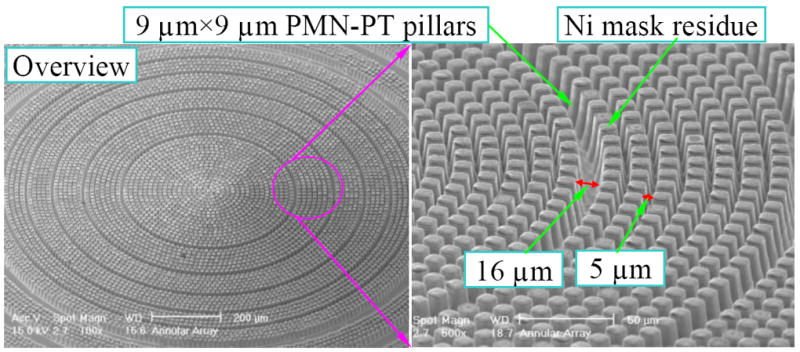
PMN-PT 1-3 composite structures by dry etching (The etching depth is about 30 μm, the gap between each array element is 16 μm, the pillar size is 9 μm by 9 μm, and the kerf between each pillar is 5 μm. With the same area of each element, the width of the outer element is only about 100μm.)
After the dry etching process, the kerfs were filled with an epoxy, Epotek 301 (Epoxy Technology, Bellerica, MA). Once the epoxy was fully cured, the surface was lapped down to the PMN-PT level. The sample was then cleaned, and a 500 Å/1500 Å Cr/Au metal layer was deposited onto the lapped surface of the sample by a sputtering machine (NSC-3000 Sputter Coater, Nano-Master, Inc., Austin, TX 78741). After the sputtering step, electrodes for a 6-element annular array were patterned using photolithography; a separation of 16 μm between each element was generated. On the other side of the sample, the PMN-PT substrate was lapped to the desired thickness (~25 μm for a 50 MHz transducer).
As mentioned above, adding backing material directly to the transducer was a better choice for high frequency transducers. A silver conductive epoxy, E-solder 3022, (VonRoll Isola, Inc., New Haven, CT 06505) was selected as the backing material for the array. Insulating structures were built along the gaps between elements using photolithographic techniques. These structures also served as molds for the conductive backing material to be filled in. As illustrated in Fig. 1, after annular array electrodes at the backside of the transducer were patterned, a negative photoresist SU-8 100 (Microchem, Inc., Newton, MA) was spin coated onto the surface at the speed of 1500 rpm for 30 seconds to a thickness of ~200 μm. The SU-8 layer was pre-baked on a hotplate for 15 minutes at 65 °C followed by 2 hours at 96 °C [15]. The sample was allowed to cool down slowly. UV radiation exposure was performed with an aligner (Karl Suss MA6 Mask Aligner, Suss MicroTec, AG, Germany). Post-exposure baking was carried out on a hotplate for 30 minutes at 96 °C. Finally, the sample was developed in SU-8 developer, PGMEA (1-methoxy 2-propyl acetate, Aldrich, Inc.). During developing, an in-house 1.2 MHz ultrasonic cleaner was used to agitate the solution to facilitate the process. Conductive backing material E-solder 3022 was then poured into the SU-8 molds, and the sample was subsequently placed in a vacuum chamber for 5 minutes. The sample was centrifuged at 3000 rpm for 10 minutes to improve the conductivity of E-solder and increase its acoustic impedance and attenuation. The conductive epoxy was left to cure overnight at room temperature. The extra E-Solder out of the insulating mold was then lapped away. Fig. 3 shows the insulating structures, a top view of the mold filled with E-solder and a cross-section view of the transducer stack with backing material included. The final thickness of the backing material was about 200μm, which is good enough to attenuate the signal down to more than 60 dB according to the simulation.
Fig. 3.
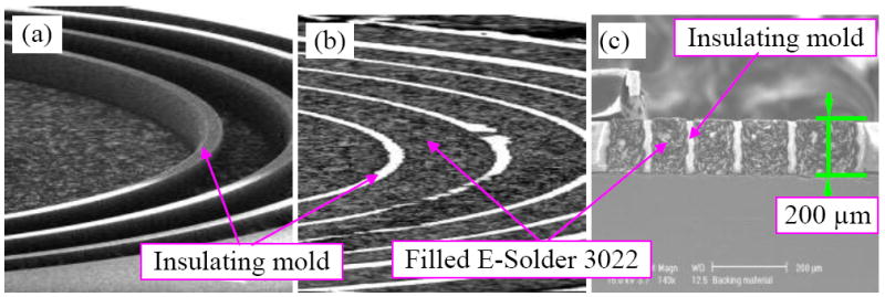
The process of attaching conductive backing material to the annular array. (a) Insulating structures fabricated onto the backside of the annular array, (b) conductive backing material fills the insulating mold, and (c) cross-sectional view of the transducer after backing material is applied.
After the mold was filled with E-solder, the annular array transducer stack was ready for assembly. From top to bottom, the acoustic stack consisted of the top electrode used as a ground, PMN-PT/epoxy 1-3 composite, backside separated annular electrodes, insulating structures, and the conductive backing material. The acoustically lossy E-solder served as a backing material, and at the same time its good electrical conductivity facilitated electric connections from individual array elements to the external electronic system.
3.2 Electrical Interconnection
The fact that the E-solder is conductive and relatively soft allows a different approach for electrical interconnection to be adopted. A new methodology for electrical interconnection in array transducers is presented here. The basic concept entails the use of ring wires (one for each of the six array elements) that are fabricated on an electric connection board (ECB). The wires are embedded under an insulating material and are routed to connection pads. On each ring wire, there are several tiny metal pins/needles extruding above the insulating layer. Following an alignment process, the needles can be easily pressed into E-solder at the backside of the array transducer, and thus the electric interconnection between ECB and each array element can be realized.
Fig. 4 shows the pictures of the fabricated ECB. On a cleaned glass substrate, a 100 Å/2500 Å Cr/Au metal layer was deposited. Corresponding to the layout of the array elements, ring wires with traces extended to connection pads were patterned using photolithography. A layer of 30 μm SU-8 was coated onto the glass and, with the standard SU-8 procedure mentioned above, was patterned, forming holes with an exact diameter of 20 μm onto the ring wires. Nickel was electroplated to fill the holes. Then the SU-8 structures were partially removed with 10 μm thick SU-8 left as an insulating layer. At the same time, the plated nickel parts in the holes were exposed to form the needles. This connection design had excellent reliability. There are at least six nickel needles corresponding to each annulus, and the loss of one or two needles does not significantly impact the interconnection between the element and the ECB.
Fig. 4.
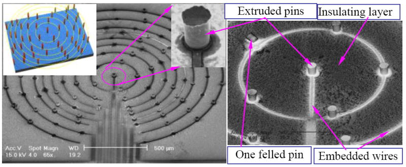
Electric connection board (ECB) for annular arrays (The height of the nickel pin is about 20 μm. There are at least 6 pins corresponding to each array element, which can guarantee the reliability of the connection. Just as illustrated in the figure, even there is one pin fell, this ECB is still can be used.)
3.3 Assembly and Packaging
After the annular array transducer stack and the ECB were fabricated, they were ready for assembly. With the help of a microscope, the two components were aligned with each ring of the ECB corresponding to each annulus of the transducer. Upon the application of suitable pressure, the Ni needles on the ECB were inserted into the backing material, E-Solder 3022, on the backside of the annular array transducer. Coaxial cables were manually soldered onto the connection pads of the ECB, and SMA connectors were attached to the other end of each cable (48 AWG, 0.0065″ in diameter, Precision Interconnect, Portland, OR.)
A cylindrical brass housing was placed concentrically around the above system, and the ground electrodes of all elements were attached to the housing. The transducer housing was then filled using an insulating epoxy, Epotek 301. Fig. 5 shows a photograph of the completed transducer.
Fig. 5.
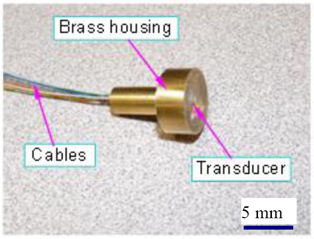
Photograph of a completed annular array transducer probe
Finally, an 8 μm layer of parylene (Parylene Deposition Unit Model PDS 2010, Specialty Coating System, Inc., Indianapolis, IN 46278) was deposited on the front of the transducer as an acoustic matching layer to improve the coupling of the transducer to water and increase the system bandwidth. The transducer was ready for characterization. The pulse/echo response, data on the insertion loss and crosstalk, and wire phantom images were acquired.
4. EXPERIMENTAL RESULTS
The transducer was tested in a degassed, deionized water bath in pulse/echo mode by reflecting the signal off an X-cut quartz target, which was 5 mm away from the testing array. To measure the pulse/echo response of the transducer, we used a Panametric pulser/receiver (Model 5900PR, Panametrics, Waltham, MA), which had a bandwidth of 200 MHz. The transducer was not electrically matched. The reflected waveforms were received and digitized by a 500 MHz oscilloscope (LC534, Lecroy, Chestnut Ridge, NY) set to 50 Ω coupling. Further information on the experimental setup can be found in Ketterling et al [2] and Snook et al. [16]. The measured pulse/echo waveforms are displayed in Fig. 6. The measured results show that the central frequency of a representative element was about 50 MHz, and the -6 dB bandwidth as wide as 90%. The insertion loss was measured using the same approach reported by Sherar and Foster [17]. The crosstalk for the adjacent elements was also measured. The average insertion loss at the central frequency of ~50 MHz was about -19.5 dB and the crosstalk between adjacent elements -35 dB. The measured pulse/echo responses of all the 6 elements were summarized and shown in Table 3. It can be seen clearly in this table that the center element had the highest peak amplitude as it was expected due to the geometry. With the width of the ring element became narrower, the amplitude of the signal became lower. Also due to lower amplitude of the signal received from outer ring elements, -6 dB pulse length became quite longer.
Fig. 6.
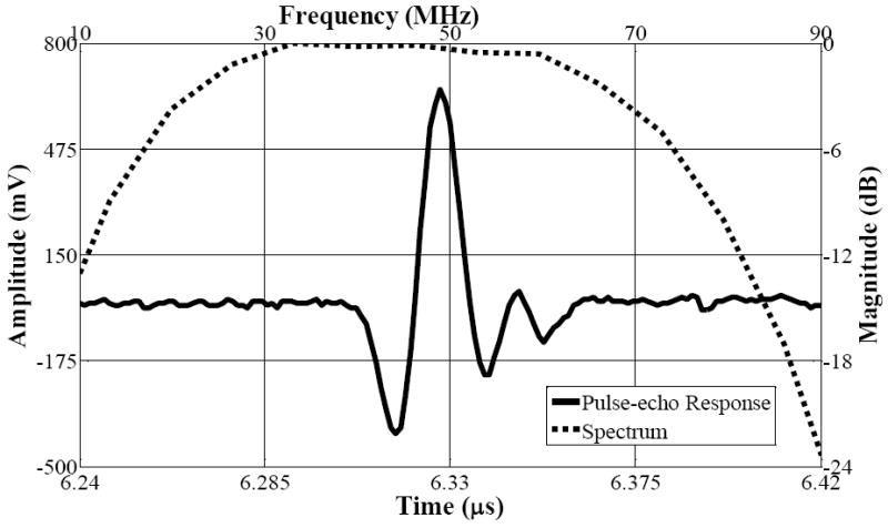
Time domain pulse/echo response and normalized frequency spectrum of the first element of the annular array.(The X-cut quartz target was about 5 mm away from the array; The -6dB bandwidth of the signal is 90%.)
Table 3.
The measured pulse echo characteristics for all annular array elements at distance of 2.8 mm
| Element No. | Central frequency (MHz) | -6 dB bandwidth (%) | Vpp (mV) | -6 dB pulse length (ns) |
|---|---|---|---|---|
| 1 | 50.0 | 90.0 | 688 | 19.5 ± .01 |
| 2 | 48.0 | 91.3 | 596 | 19.4 ± .04 |
| 3 | 47.6 | 92.0 | 425 | 1.9.4 ± .04 |
| 4 | 47.0 | 90.6 | 316 | 19.6 ± .02 |
| 5 | 48.0 | 87.6 | 302 | 19.5 ± .02 |
| 6 | 49.0 | 92.5 | 278 | 20.0 ± .05 |
The electric impedance of the composite material was also measured and the coupling factor kt was calculated. The value of kt is 0.82 which was much higher than that of the single crystal PMN-PT (0.58). A wire phantom was initially used to assess the array performance. The phantom consisted of five 25 μm wires spaced at 1 mm in depth and 0.25 mm lateral intervals. The transducer was scanned across the wire phantom with the first wire 1 mm away from the surface of the transducer. Each element was pulsed and used for reception, respectively. The dynamic range was 40 dB. Fig. 7 shows an example of data taken from the wire phantom by using the first array element. The experimental results demonstrate the imaging performance of the transducer without dynamic focusing or beamforming.
Fig. 7.
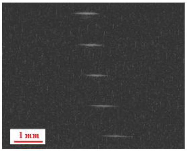
B-mode image of a wire phantom obtained by mechanically scanning the annular array across the phantom by using the first array element. The image dimensions are about 5 mm by 5 mm, and the transducer was located on the top of the image (distance from the first wire is 1 mm and from the last one is 5 mm). The dynamic range of the image is 40 dB.
5. SUMMARY AND CONCLUSIONS
The development of high frequency ultrasound array transducers for medical imaging is critically dependent on fabrication methods for producing small array elements with fine kerfs. This paper reports micromachining techniques that have been developed and can be used in producing a variety of high frequency ultrasonic array transducers. This is the first report that a PMN-PT/epoxy 1-3 composite high frequency annular array transducer (50 MHz) has been designed and fabricated in such a way. Spurious lateral modes in these composites were suppressed by a random layout of the PMN-PT pillars in the composite material. The conductive backing material was attached to the transducer directly, which could dramatically improve the bandwidth and sensitivity of the array transducer. Furthermore, a new needle electric connection strategy was proposed and successfully implemented. It can be applied to other array transducers that have fine elements and narrow pitches as well. The central frequency of the array fabricated was 50 MHz and the -6 dB bandwidth about 90%.
Highlights.
>We made high frequency PMN-PT/epoxy 1-3 composite ultrasonic annular arrays. >A novel electrical interconnection strategy for density array was implemented. > The micromachining techniques are promising for making high frequency transducers.
Acknowledgments
The authors acknowledge processing help from Jay Williams. Helpful discussions with Dr. Jonathan M. Cannata are also gratefully acknowledged. The authors also acknowledge support from the NIH under Grant CA110214-02 and P41-EB2182.
Footnotes
Publisher's Disclaimer: This is a PDF file of an unedited manuscript that has been accepted for publication. As a service to our customers we are providing this early version of the manuscript. The manuscript will undergo copyediting, typesetting, and review of the resulting proof before it is published in its final citable form. Please note that during the production process errors may be discovered which could affect the content, and all legal disclaimers that apply to the journal pertain.
References
- 1.Brown JA, Démoré-Morton CE, Lockwood GR. Design and fabrication of annular arrays for high-frequency ultrasound. IEEE Trans Ultrason Ferroelect Freq Contr. 2004;51(no 8):1010–1017. doi: 10.1109/tuffc.2004.1324405. [DOI] [PubMed] [Google Scholar]
- 2.Ketterling JA, Aristizábal O, Turnbull DH, Lizzi FL. Design and fabrication of a 40 MHz annular array transducer. IEEE Trans Ultrason Ferroelect Freq Contr. 2005;52(no 4):672–681. doi: 10.1109/tuffc.2005.1428050. [DOI] [PMC free article] [PubMed] [Google Scholar]
- 3.Gottlieb EJ, Cannata JM, Hu CH, Shung KK. Development of a high-frequency (> 50 MHz) copolymer annular-array, ultrasound transducer. IEEE Trans Ultrason Ferroelect Freq Contr. 2006;53(no 5):1037–1045. doi: 10.1109/tuffc.2006.1632693. [DOI] [PubMed] [Google Scholar]
- 4.Smith WA, Shaulov AA, Auld BA. Design of piezocomposites for ultrasound transducers. Ferroelectrics. 1989;91:155–162. [Google Scholar]
- 5.Cannata JM, Williams JA, Zhou Q, Ritter TA, Shung KK. Development of a 35-MHz piezo-composite ultrasound array for medical imaging. IEEE Transactions on Ultrasonics, Ferroelectrics, and Frequency Control. 2006;53(No 1) doi: 10.1109/tuffc.2006.1588408. [DOI] [PubMed] [Google Scholar]
- 6.Liu R, Knapik D, Harasiewicz KA, Foster FS, Flanagan JG, Pavin CJ, Trope GE. Fabrication of 2-2 piezocomposites by interdigital pair bonding. Proc IEEE Ultrasonics Symposium. 1999;2:973–976. [Google Scholar]
- 7.Snook K, Hu CH, Shrout T, Shung KK. High-frequency ultrasound annular-array imaging. Part I: array design and fabrication. IEEE Transactions on Ultrasonics, Ferroelectrics, and Frequency Control. 2006;53(No 2):300–308. doi: 10.1109/tuffc.2006.1593368. [DOI] [PubMed] [Google Scholar]
- 8.Chabok H, Cannata J, Kim H, Shung K. Development of high frequency annular array ultrasound transducers using interdigital bonded composites. IEEE International Ultrasonics Symposium Proceedings. 2009:2708–2711. [Google Scholar]
- 9.Jiang X, Yuan JR, Cheng A, Snook K, Cao P, et al. Microfabrication of piezoelectric composite ultrasound transducer (PC-MUT) IEEE International Ultrasonics Symposium Proceedings. 2006:918–921. [Google Scholar]
- 10.Liu CG, Wu DW, Zhou QF, Djuth FT, Shung KK. High-frequency (50-100MHz) medical ultrasound transducer arrays produced by micromachining bulk PZT materials. IEEE International Ultrasonics Symposium Proceedings; Beijing, China. 2008. pp. 690–693. [Google Scholar]
- 11.Davidsen RE, Smith SW. Two-dimensional arrays for medical ultrasound using multilayer flexible circuit interconnection. IEEE Transactions on Ultrasonics, Ferroelectrics, and Frequency Control. 1998 Nov;45(No 2):338–348. doi: 10.1109/58.660144. [DOI] [PubMed] [Google Scholar]
- 12.Martha Grewe, Gururaja T, Shrout TR, Newngam R. Acoustic properties of particle/polymer composites for ultrasonic transducer backing applications. IEEE Transactions on Ultrasonics, Ferroelectrics, and Frequency Control. 1990 Nov;37(No 6):506–514. doi: 10.1109/58.63106. [DOI] [PubMed] [Google Scholar]
- 13.Jensen JA. Users’ guide for the Field II program. 2001 [Google Scholar]
- 14.Wu DW, Liu CG, Zhou QF, Shung KK, Djuth FT. High-frequency micromachined ultrasonic annular arrays. IEEE International Ultrasonics Symposium Proceedings. 2009:2201–2204. [Google Scholar]
- 15.Microchem, Inc., Negative tone photoresist formulations 50-100.
- 16.Snook KA, Zhao JZ, Alves CH, Cannata JM, Chen WH, Meyer RJ, Jr, Ritter TA, Kirk Shung K. Design, fabrication, and evaluation of high frequency, single-element transducers incorporating different materials. IEEE Trans Ultrason Ferroelect Freq Contr. 2002;49(no 2):169–176. doi: 10.1109/58.985701. [DOI] [PubMed] [Google Scholar]
- 17.Sherar MD, Foster FS. The design and fabrication of high frequency poly(vinylidene fluoride) transducers. Ultrason Imag. 1989;11:75–94. doi: 10.1177/016173468901100201. [DOI] [PubMed] [Google Scholar]


