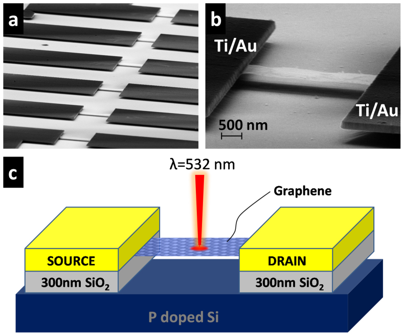
Figure 1. CVD-grown graphene photodetector devices.
(a) SEM images showing an array of fully suspended graphene photodetectors fabricated on large area CVD graphene on a 300 nm layer of SiO2thermally grown on p-type silicon substrate. (b) SEM image of individual photodetector device with well suspended graphene microribbon contacted with Ti/Au metal contacts on both sides. (c) Schematic of the suspended graphene device during the photocurrent measurements.

