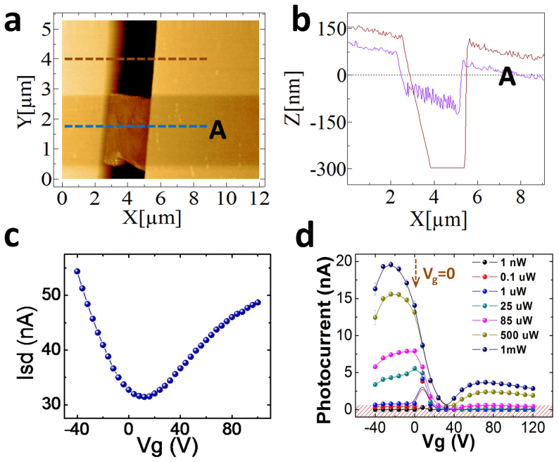
Figure 2. Structural, electronic, and optoelectronic characterization of the graphene photodetector devices.
(a) AFM scans over a suspended graphene ribbon. (b) Corresponding height map showing that the suspended graphene area is about 250 nm above the silicon substrate. (c) Backgate sweep without light at constant source drain bias of 5 mV showing Dirac point near +15 V indicating slight p-type graphene. Data recorded after current annealing for several hours and stable response. (d) Photocurrent measured on the fully supported graphene microribbon with varying backgate at different incident powers. The hashed region illustrates the instrument noise floor of about 50 pA.

