
Figure 1.
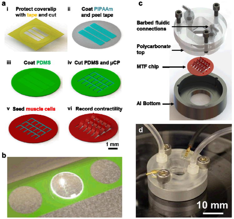
Higher throughput heart on a chip and fluidic microdevice. (a) A schematic of fabrication process (i) A glass coverslip is covered with protective tape and PIPAAm islands are cut into by an engraving laser and peeled using a sharp tweezer. (ii) A thin layer of PIPAAm is spun coat, (iii) the tape is removed and PDMS is spun coat. (iv) The boundaries of thin films are then cut into the PDMS and peeled. (v) The chip is then ready for micro contact printing of fibronectin and cell seeding. (vi) Upon PIPAAm dissolution, individual MTFs are released from the surface and interrogated optically. (b) Image of the engraving laser processing MTFs in an 18 mm diameter chip. A batch of multiple chips can be fabricated by this computer aided design process. (c) Exploded view of the conception and assembly of a fluidic device which fits an 18 mm chip. The device consists of an aluminum bottom with a recess to hold the chip, a transparent polycarbonate top held in place by three screws and barbed fittings for fluidic input and output. (d) Image of an actual device in action. The connection for electrical field stimulator can also be seen in addition to the fluidic tubing.