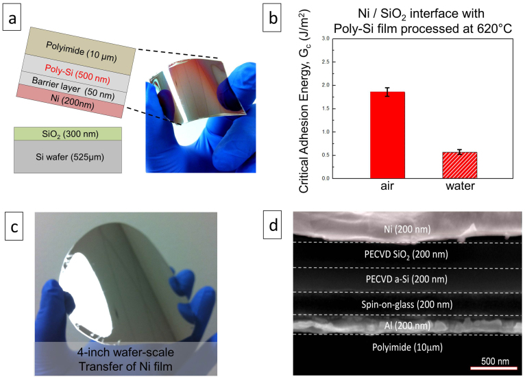
Figure 5. Important features of the peel-and-stick process.
(a) A schematic (left) of the peel-and-stick process to transfer the poly-Si film processed at 620°C onto a flexible polyimide substrate directly deposited on top. An optical image (right) of the clean and defect-free surface of the poly-Si film after the peel-and-stick process. (b) Critical adhesion energy (Gc) of Ni-SiO2 interface in air with a 20% relative humidity and in water at 21°C for the particular case of transferring the poly-Si film. (c) An optical image of a 4-inch wafer-scale transferred Ni film from a SiO2/Si wafer onto a flexible plastic substrate. (d) A SEM image of the transferred 6-layer-stacked thin-films from a SiO2/Si wafer to a flexible plastic substrate.

