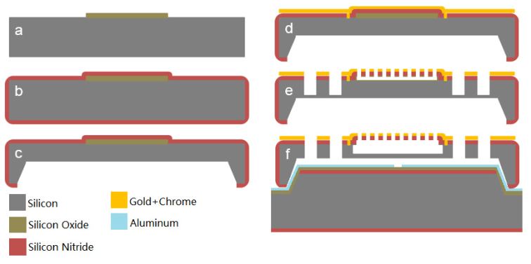
Fig. 2.

Fabrication process flow for the micromirror. (a) Silicon oxide pads are deposited and patterned. (b) LPCVD silicon nitride deposition. (c) Backside KOH etch. (d) Vias are created and the surface is metallized. (e) Pattern the metal layers and transfer the pattern into the nitride layer using RIE. Trenches are etched with DRIE. (f) Final release in HF and KOH, and align with the bottom electrode wafer.
