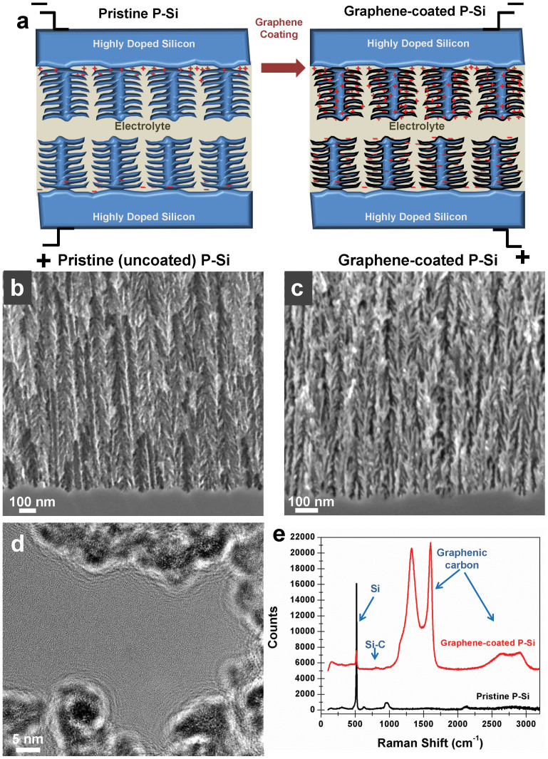
Figure 1. Graphene coating on porous silicon.
(a). Scheme of the effect of coating P-Si on the capacitive charge storage properties. SEM cross-sectional images of porous silicon showing the interface between the etched porous silicon and the silicon wafer for the case of (b). uncoated, pristine porous silicon and (c). graphene coated porous silicon. (d). Cross-sectional TEM image of graphene-coated porous silicon structures (scale bar = 5 nm). (e). Raman spectroscopy taken at 785 nm showing pristine P-Si and graphene-coated P-Si, with the carbon, Si, and Si-C peaks labeled.

