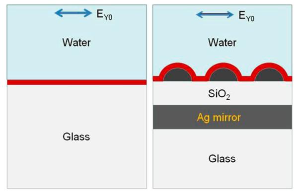
Figure 2.
Schemes of multilayer and reference models used for numerical calculations with parameters: Ag array of semispheres with diameter of 60 and 40 nm edge-to-edge spacing, Ag mirror with thickness of 200 nm, SiO2 layer with variable thickness from 0 to 240 nm, and water thickness of 500 nm. The average excitation field intensity and radiation power of randomly distributed dipoles were performed using the entire volume of a layer of 10 nm above the silica (or glass) surface. The arrow shows the polarization of incident electrical field.

