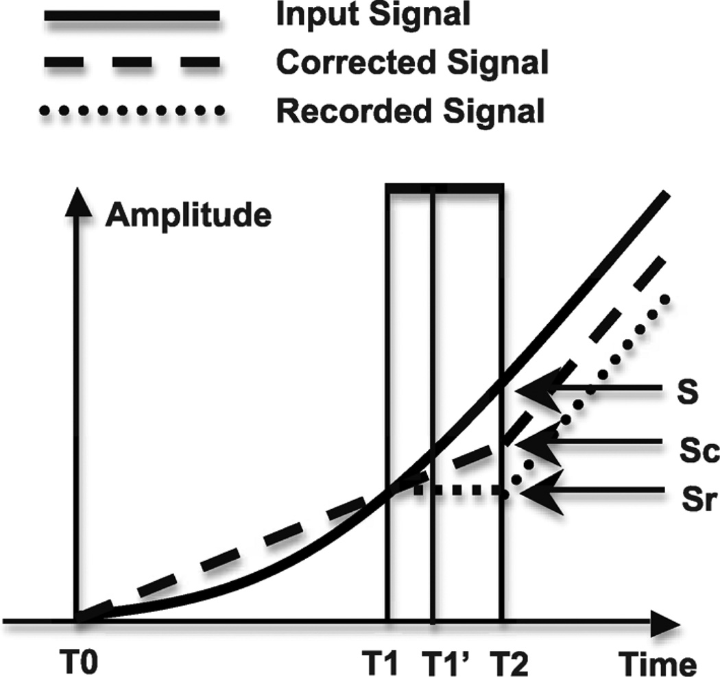
Fig. 3.
Loop delay induced sampling noise in fixed window level crossing ADC. The previous pulse ends at TO, the current pulse starts at T1’ and finishes at T2. T1 to T1’ is the propagation delay of the comparator. The input signal between T1 and T2 will be lost. The amplitude between S and Sr is the sampling noise. The sampling noise can be partially compensated in the digital domain by estimating the slope of the input signal using extrapolation from the previous pulse, as shown as Sc. The sampling error can be reduced by implementing delta modulator with shorter loop delay.

